DeepTouch1000

Products and engineering

Assembly, test, cleaning and storage

Browse by probe card process, or open the specifications for PCT5801, DeepTouch1000, the high-pin-count socket tester and EVA100.

PRODUCT LINES

Two product lines

One is built around making and proving MEMS probe cards; the other starts from the UF200 information box, giving installed probers the data layer and EAP interfaces a modern fab expects, and extends into retrofit and pre-owned equipment. Each line has a clickable workshop.

Line position

From needle cutting to storage: which tools on this chain are ours

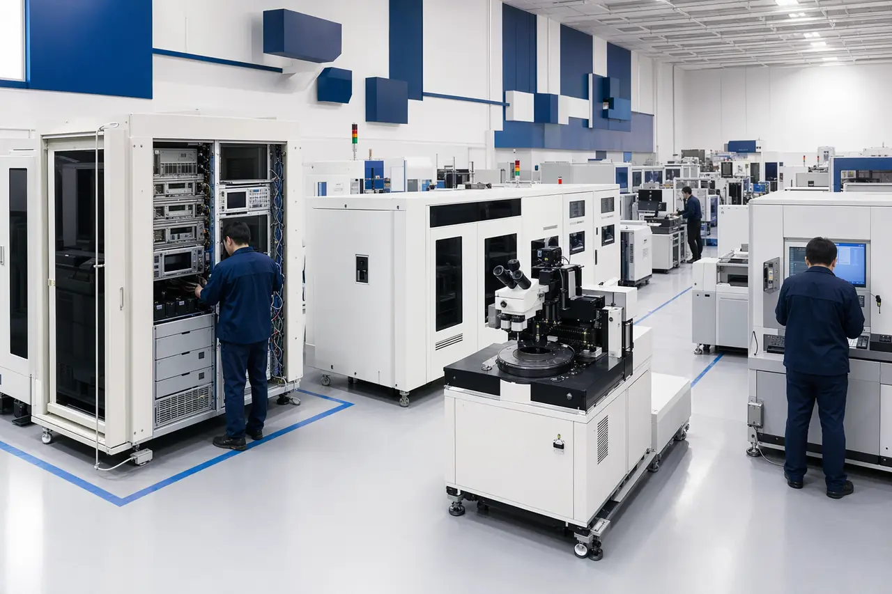
The cost of a probe card rarely stops at purchase: assembly consistency, post-clean residue, storage environment, test criteria — wherever a line lacks the equipment for one of these, the problem surfaces later, in volume production. This MEMS probe-card manufacturing and validation cleanroom lays out the whole chain by its real process bays and marks which parts our equipment covers and which are left to specialist suppliers. Click any tool to zoom in on what it does and the product behind it; the two ends of the room are incoming and shipping.

Enter the line
Prober informatization and pre-owned equipment

Bringing installed probers up to what a modern fab or OSAT asks of them

The UF200 is a machine of the 1990s and the UF3000 of the 2000s. When they left the factory, no line asked for barcode or QR scanning, RFID handover, or MES and EAP connectivity - the machines are not broken, they were simply born before those requirements existed. Today those requirements are the price of entry to a modern fab or OSAT, and machines that can still do the work get replaced whole because of them. Our answer is to bring the old machine back to life: upgrade rather than scrap. With the UF200 information box at the centre we add that layer, software through hardware - the prober itself is untouched, what it already knows is read out and carried into the plant's systems - and from there we extend to scanning and lot traceability, EAP and automated material flow, modern-factory retrofit, with refurbished probers, testers and parts underneath it all. This CP bay, modelled on the actual machines, is where that lands: the four boards on the wall are real screens from the information box, and the six probers and four docking cells set out the range we can take on.

Enter the line
Memory and HBM

The device sets the pin count, not us

From NAND, NOR and DRAM through to HBM, the touchdown is the same and the pin count differs by almost twenty times. Chuck force and the PCT5801v2 architecture are designed around the top of that range; the current PCT5801 configuration is 67,000 pins. These are pins on the card, which is not the same quantity as the tester channel counts in the specifications.

01 / ASSEMBLY

MEMS probe card assembly

Build the station around the probe, substrate, fixture, vision alignment, recipes and post-assembly validation.

Configuration: probe type, substrate, datum, accuracy, takt and acceptance method.

Fixture and changeover

Design holding, datum and changeover for the probe, substrate and assembly process.

Vision-assisted alignment

Confirm placement and retain process and exception images.

Recipe and traceability

Record work order, material, operator, recipe version and result.

Post-assembly validation

Connect AOI, XYZ, Pin Force and electrical checks.

02 / ELECTRICAL + PHYSICAL TEST

PCT5801 and DeepTouch1000

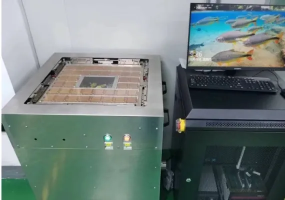
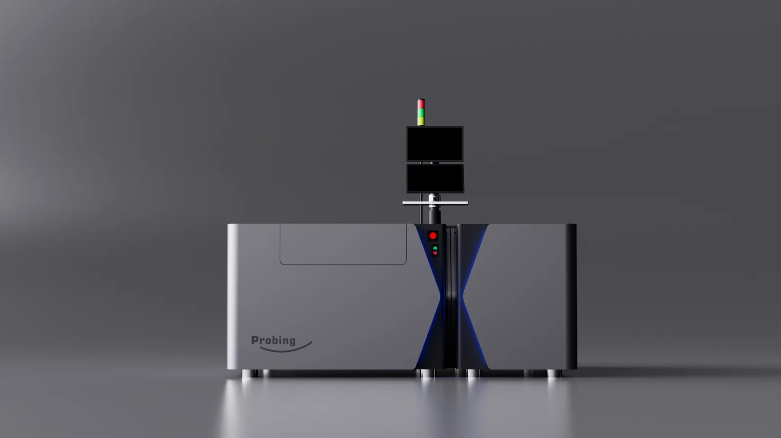
PCT5801 handles the end-to-end electrical path; DeepTouch1000 delivers 1000 kgf whole-card touchdown with 3D probe-tip inspection.

Pin ceilings: PCT5801 at 67,000 pins, v2 targeting 300,000 pins; DeepTouch1000 at 1000 kgf chuck force and up to 300,000 pins.

Open / Short / Leakage

Continuity, shorts and nA-level leakage against a 10 nA threshold; task times are agreed in the technical agreement.

Control resources

MCW, Relay, FPGA, ASIC, SPI and I²C checks.

High-channel expansion

1,024-channel modules are combined for the motherboard and tester.

Physical validation

Load, probe-tip XYZ, probe marks and contact state support electrical anomaly analysis.

03 / CLEAN + REINSPECT

Probe card cleaning and reinspection

Manage atomized IPA, controlled brushing, clean gas and three-direction image review by recipe.

Configuration: probe type, material compatibility, particle limits, rework conditions and task time.

Atomized IPA

Set delivery range and process parameters for the card.

Controlled brushing

Manage brush type, movement, contact and cycle count.

Clean-gas blowoff

Establish a stable state for reinspection and electrical test.

Three-direction review

Retain images, judgement and rework history.

04 / CONTROLLED STORAGE

Traceable probe card storage

Manage receipt, issue, return and inventory through environment control, RFID and factory-system interfaces.

Configuration: capacity, environment, RFID, WMS/EAP/MES, handoff method and store/retrieve time.

Controlled environment

Set nitrogen, ESD, temperature/humidity and alarms for the card and facility.

RFID identity

Link card ID, location, state and movement history.

WMS / EAP / MES

Receive tasks and return state, exception and audit records.

Manual or automated handoff

Configure manual, AMR, robot or OHT handling.

OTHER EQUIPMENT AND SERVICES

Sockets, EVA100 and surplus equipment

High-pin-count socket testers, EVA100 test-program development and surplus semiconductor equipment are listed here.

High-pin-count package socket test equipment

PSTA20K Ultra-High-Channel Socket Tester

A socket tester built on an Advantest EVA100 front end, fanned out through a relay matrix and a custom motherboard, for open, short, leakage and per-pin contact resistance on high-pin-count package sockets.

View full details
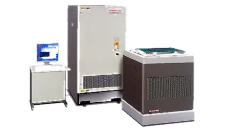
Semiconductor test system equipment visual (not an actual EVA100)

Advantest EVA100 Application and Test Engineering

Advantest EVA100 digital and mixed-signal test system: 128-1024 digital channels, per-pin PPMU/PDPS, 1000 V HVI, 500 MHz scope, with Probing application engineering.

View full details
Portfolio illustration of surplus lithography, prober and test equipment

Surplus Semiconductor Equipment and Engineering

Scope covering ASML lithography, Accretech/TEL probers and Advantest ATE, with inventory, configuration, logistics and installation confirmed per unit.

View full details
EQUIPMENT INFORMATION

One page per machine

Each page lists applications, specifications, operating steps, project delivery and acceptance conditions.

High-channel electrical and physical validationMemory Probe Card Test SystemA probe card validation platform for HBM and high-pin-count applications, combining Open, Short, nA-level leakage, control resources and physical inspection.A test system, not a probe card analyzerPCT5801 Probe Card Test System16,384-channel standard configuration delivered (65,536 maximum); current platform capacity 67,000 card-side pins; the next-generation PCT5801v2 targets 300,000 pins. Covers open, short, 10 nA leakage, control resources and TDR.The board between the card and the testerProbe Card MotherboardsProbe card motherboards designed and built as ODM for the tester platform and card type, covering 8 TOM, 32 TOM, FULL, SSV/XV and 4,000-pin configurations with DC and TDR AC test.1000 kgf full-load measured · for cards to 300,000 pinsDeepTouch1000 Probe Station for Probe Card TestA dedicated probe station for whole-card validation at high pin counts: 1000 kgf chuck force (full-load measured) for target cards to 300,000 pins, PB5801 all-in-one structure and 3D probe-tip inspection linked to PCT5801 results.Pick · align · weld · closed-loop verificationMEMS Probe Card Pin Assembly and Laser Micro-WeldingPin assembly and laser micro-welding equipment for MEMS probes and substrates: three-gripper handover, alignment stage, autofocus post-weld inspection, closed with PCT5801 electrical test and DeepTouch1000 whole-card validation.Atomized IPA, controlled brushing, clean gas and closed-loop reviewProbe Card Cleaning and Three-Direction ReinspectionControlled probe card cleaning with atomized IPA, controlled brushing, clean-gas blowoff, three-direction image review and RFID traceability.Controlled environment, RFID and factory interfacesTraceable Probe Card Storage SystemControlled probe card storage with nitrogen/ESD, RFID, WMS/EAP/MES interfaces and manual, AMR, robot or OHT handoff.EVA100 plus relay matrix · beyond 5,000 channelsPSTA20K Ultra-High-Channel Socket TesterA socket tester built on an Advantest EVA100 front end, fanned out through a relay matrix and a custom motherboard, for open, short, leakage and per-pin contact resistance on high-pin-count package sockets.Digital and mixed-signal test system · E-Model / P-ModelAdvantest EVA100 Application and Test EngineeringAdvantest EVA100 digital and mixed-signal test system: 128-1024 digital channels, per-pin PPMU/PDPS, 1000 V HVI, 500 MHz scope, with Probing application engineering.Equipment scope, condition review and project deliverySurplus Semiconductor Equipment and EngineeringScope covering ASML lithography, Accretech/TEL probers and Advantest ATE, with inventory, configuration, logistics and installation confirmed per unit.3000+ holes · no grooves · 5 μm flatnessPorous Gold-Plated Chuck TopA porous gold-plated chuck top for MOSFET testing with over 3000 dense vacuum holes, a gold-plated grooveless surface and 5 μm flatness, fitting Tokyo Seimitsu ACCRETECH APM90A and UF200/UF200A/UF200R probers.40 s boot · 250,000 dies · Chinese UIuP200A Prober Control System UpgradeA control system upgrade for Tokyo Seimitsu APM90A and UF200 series probers in service: 40 second boot, 250,000 dies per wafer, a Chinese interface, and compatibility with the original probe cards and consumables.In development · design stageECP1010 Embedded-Chip PCB Automatic Test SystemAutomatic electrical test for embedded-chip PCB: loading, vision alignment, press-down contact, built-in ATE, 1,024 channels expandable to 16,384. Design-stage product.Image sensor test · solution stageCMOS Image Sensor Test SolutionThe bottleneck in image sensor test is moving the data: on the EVA100 platform each site carries its own APU image board, so the algorithm runs locally and sites never wait for each other. MIPI CSI-2 / DVP capture across RGB, YUV and RAW.Engineering · barcode in, rules appliedProber Barcode Entry and LOT HandlingA USB scanner feeds the prober's native barcode port through a relay; a rule engine extracts and validates the LOT. In-house engineering project.Engineering prototype · bolt-on acquisitionProber Information BoxA bolt-on unit that leaves the prober untouched and reads wafer geometry, test counters and probe-card counts from the machine itself. Engineering prototype.