Pre-owned probers and the testers they dock to, in one hall
A digital twin of a CP bay modelled on the actual machines: six probers along the north side - TSK APM90A, UF200, UF3000, UF3000ex, AP3000 and the TEL P-12XL - and four test cells facing them: docking cells for the Advantest V93000, the Advantest T5833 and the Teradyne M5, plus a cable-connected Advantest EVA100. The four production boards on the wall are real screens from our own information box. Click any machine or board and the detail appears below.
8 Available · 3 Serviced · 1 Under improvement · 5 Engineering prototype
Drag to orbit · scroll to zoom · click a machine or board
Click any machine, or a production board on the wall, and the detail appears here.
Available
01 · APM90A (TSK, 200 mm)
Control-system upgrade for a legacy platform
The Tokyo Seimitsu APM90A is the generation before the UF200: a 200 mm fully automatic prober installed across Korea, Japan and Taiwan between 1994 and 1997. As built it boots in about 180 seconds, runs an English/Japanese interface, moves data on floppy disks and handles about 60,000 dies per wafer. What we do with this generation is a control-system upgrade: about 40 seconds to boot, 250,000 dies per wafer, a full Chinese interface, and continued compatibility with the original probe cards, consumables and data formats. The maker’s plate reads A-PM-90A.
Surplus Semiconductor Equipment and Engineering
Scope covering ASML lithography, Accretech/TEL probers and Advantest ATE, with inventory, configuration, logistics and installation confirmed per unit.
A control system upgrade for Tokyo Seimitsu APM90A and UF200 series probers in service: 40 second boot, 250,000 dies per wafer, a Chinese interface, and compatibility with the original probe cards and consumables.
The TSK 200 mm workhorse installed from 1998 onwards: 125/150/200 mm wafers, 5 µm overall accuracy, a nickel or gold plated heatable 200 mm chuck, GPIB/TTL interfaces, roughly 70 seconds to boot and up to 100,000 dies per wafer. We rebuild the whole machine to UF200A specification in our Wuxi plant with every function enabled and the software version the customer asks for. The native interface is English/Japanese; the Chinese-language operating system is our own. Hot and cold chucks, wafer ID OCR, round or square needle cleaners, inking units and remote operation can be added.
Surplus Semiconductor Equipment and Engineering
Scope covering ASML lithography, Accretech/TEL probers and Advantest ATE, with inventory, configuration, logistics and installation confirmed per unit.
A control system upgrade for Tokyo Seimitsu APM90A and UF200 series probers in service: 40 second boot, 250,000 dies per wafer, a Chinese interface, and compatibility with the original probe cards and consumables.
A USB scanner writes through a relay into the prober's native barcode interface, and a rule engine extracts and checks the LOT before anything reaches the machine: wrong format, wrong length or a failed check digit means nothing is sent. The length limit matches the UF200's own LOT field. This is our own project, under improvement, with no customer deliveries yet.
Prober Barcode Entry and LOT Handling
A USB scanner feeds the prober's native barcode port through a relay; a rule engine extracts and validates the LOT. In-house project under improvement.
Turning what an old machine knows into data you can hand over
A bolt-on acquisition unit that leaves the prober itself untouched: one link to the machine, one to the plant network. It reads wafer geometry, test counts and cumulative probe-card touchdowns and cleaning cycles from the machine's own configuration card and running memory, and brings the screen to a browser. Every page states the grade of its source, and a page whose source cannot be established locks itself rather than showing an invented number. Engineering prototype: it runs continuously on our own engineering machine and has not been delivered to a customer.
Prober Information Box
A bolt-on unit that leaves the prober untouched and reads wafer geometry, test counters and probe-card counts from the machine itself. Engineering prototype.
The ACCRETECH 300 mm platform built from 2005, handling both 200 mm and 300 mm wafers: a nickel-plated heatable 300 mm chuck, automatic card loading, automatic needle cleaning and alignment, probe-mark inspection, 200 kg of standard chuck force (300 kg optional) and a published overall accuracy of ±2 µm. We rebuild the machine, re-verify its parameters and install it on site; refurbished stock covers both ambient and hot/cold configurations.
Surplus Semiconductor Equipment and Engineering
Scope covering ASML lithography, Accretech/TEL probers and Advantest ATE, with inventory, configuration, logistics and installation confirmed per unit.
The high-force member of the UF3000 family: 300 kg of chuck force as standard and 400 kg as an option, for probe cards with high pin counts and heavy contact force. The UF3000 is 200 kg standard with 300 kg optional, and the two must not be mixed up. It is easy to tell apart from the UF3000 by eye - an indigo stripe runs down the front-left corner with the wordmark rotated along it, the model name moves to the black gloss panel on the loader, and the big hollow blue wordmark of the UF3000 is absent from the body. Scope of work is the same: full rebuild, parameter re-verification, on-site installation, after-sales to new-machine standard. Refurbished stock covers ambient and hot/cold configurations. The machine’s own badge reads UF3000 EX.
Surplus Semiconductor Equipment and Engineering
Scope covering ASML lithography, Accretech/TEL probers and Advantest ATE, with inventory, configuration, logistics and installation confirmed per unit.
A control system upgrade for Tokyo Seimitsu APM90A and UF200 series probers in service: 40 second boot, 250,000 dies per wafer, a Chinese interface, and compatibility with the original probe cards and consumables.
ACCRETECH's current-generation 300 mm prober, published at +/-0.8 um and +/-1.5 um overall accuracy and able to run both 300 mm and 200 mm bare wafers. Single or dual loader with AMHS automation, needle cleaning, a fan-filter mini-environment, an ambient/hot chuck to 200 C, HF jig and hinge-manipulator tester interfaces and automatic card exchange are options. Above the deck opening sits a fixed bridge beam that holds the probe card and takes the docking load, and it cannot be removed - so probe-card and fixture designs have to work around it, as ours did while still meeting a cold-chuck requirement. This cell is a machine we build card and fixture solutions for; the machine itself is not on our own sales list.
Surplus Semiconductor Equipment and Engineering
Scope covering ASML lithography, Accretech/TEL probers and Advantest ATE, with inventory, configuration, logistics and installation confirmed per unit.
The Tokyo Electron 300 mm flat-top prober installed around 2004: a WAPP needle-cleaning module, SACC automatic card loading, a gold or nickel plated 300 mm hot chuck with a cold option, and probe-mark inspection. On chuck force the P-12XL is 80 kg as standard while the P-12XLn/n+ is 100 kg with a 200 kg option, so the exact variant matters when you ask for a quote. For TEL probers of 200 mm and above we provide installation, commissioning and fixture work.
Surplus Semiconductor Equipment and Engineering
Scope covering ASML lithography, Accretech/TEL probers and Advantest ATE, with inventory, configuration, logistics and installation confirmed per unit.
Test head tumbled face-down, hard-docked to the head plate
The V93000 carries its instrument cards inside the test head, so there is no large electronics cabinet: for wafer sort the manipulator tumbles the head interface-down over the prober's head plate and hard-docks it, with the probe card mounted straight onto the head interface and no pogo tower in between. A support rack beside the cell supplies power and cooling water through the thick cable bundle running to the back of the head. We supply 93000 PS400 configurations on these terms: a fully refurbished machine with a one-year warranty, and the PCI-E controller upgrade carried out on site by the equipment maker after delivery (terms as quoted in 2023; the contract governs). In this cell the head is docked onto a UF3000.
Surplus Semiconductor Equipment and Engineering
Scope covering ASML lithography, Accretech/TEL probers and Advantest ATE, with inventory, configuration, logistics and installation confirmed per unit.
Cabinet behind, prober in front, test head lying flat on top
The standard memory-test arrangement: off-white mainframe cabinets in a row along the wall, a prober in front of each one, and a flat grey test head lying face-down on the prober's head plate, fed by a thick cable bundle that leaves the cabinet low at the front and loops across the floor to the back of the head. In this family the mainframe is about 850 (W) × 1050 (D) × 1650 (H) mm and a single-tower head about 830 × 990 × 630 mm. We build our own motherboard/WMB for this platform, including 32 TOM configurations, and have run full-card verification on a UF3000. This cell is docked onto an AP3000, with the head coming down over that machine’s fixed bridge beam.
Surplus Semiconductor Equipment and Engineering
Scope covering ASML lithography, Accretech/TEL probers and Advantest ATE, with inventory, configuration, logistics and installation confirmed per unit.
PCT5801 forms an end-to-end path from full-function ATE through a relay matrix and motherboard to the probe card, covering open, short, 10 nA leakage, control resources and TDR transfer time; the v2 flagship reaches 300,000 pins.
Electronics inside the tester, docked straight to the probe card
The Magnum family integrates the test electronics inside the tester body, so there is no separate electronics cabinet. For wafer sort the K52 interface docks straight to the probe card with no pogo tower, the body pressing face-down over the prober — the same docking picture as the V93000 but with a squarer body. Our sales and service scope covers the Teradyne Magnum 5 (alongside the J750, UltraFlex and others), and our probe-card test solution supports the M5 platform. This cell shows the docking arrangement. This cell is docked onto a P-12XL.
Surplus Semiconductor Equipment and Engineering
Scope covering ASML lithography, Accretech/TEL probers and Advantest ATE, with inventory, configuration, logistics and installation confirmed per unit.
PCT5801 forms an end-to-end path from full-function ATE through a relay matrix and motherboard to the probe card, covering open, short, 10 nA leakage, control resources and TDR transfer time; the v2 flagship reaches 300,000 pins.
A small box on a stand, one flat cable up to the prober
The EVA100 is a benchtop test unit: the standard unit is 363 (W) × 472 (D) × 206 (H) mm and 8.2–19.4 kg, a black chassis with a magenta front frame and an open card cage on top. Two official docking kits exist — a fixture that hangs the unit straight under the head plate, or the cable connection shown here, where the unit sits on a stand beside the prober and a flat cable bundle runs from the performance-board area on top of the unit to a Cable Connection PB plugged into the prober's card holder. We use the EVA100 as the test front end for socket and probe-card test solutions. The EVA100 in this cell is cabled to a UF200.
Advantest EVA100 Application and Test Engineering
Advantest EVA100 digital and mixed-signal test system: 128-1024 digital channels, per-pin PPMU/PDPS, 1000 V HVI, 500 MHz scope, with Probing application engineering.
A porous gold-plated chuck for MOSFET test: over 3,000 densely spaced vacuum holes, a gold-plated surface, no grooves, and 5 µm flatness, made to fit the chuck interface of the Tokyo Seimitsu (ACCRETECH) APM90A and the UF200/UF200A/UF200R series. After fitting we re-verify holding force, flatness and temperature distribution, and it is accepted together with the machine.
Porous Gold-Plated Chuck Top
A porous gold-plated chuck top for MOSFET testing with over 3000 dense vacuum holes, a gold-plated grooveless surface and 5 μm flatness, fitting Tokyo Seimitsu ACCRETECH APM90A and UF200/UF200A/UF200R probers.
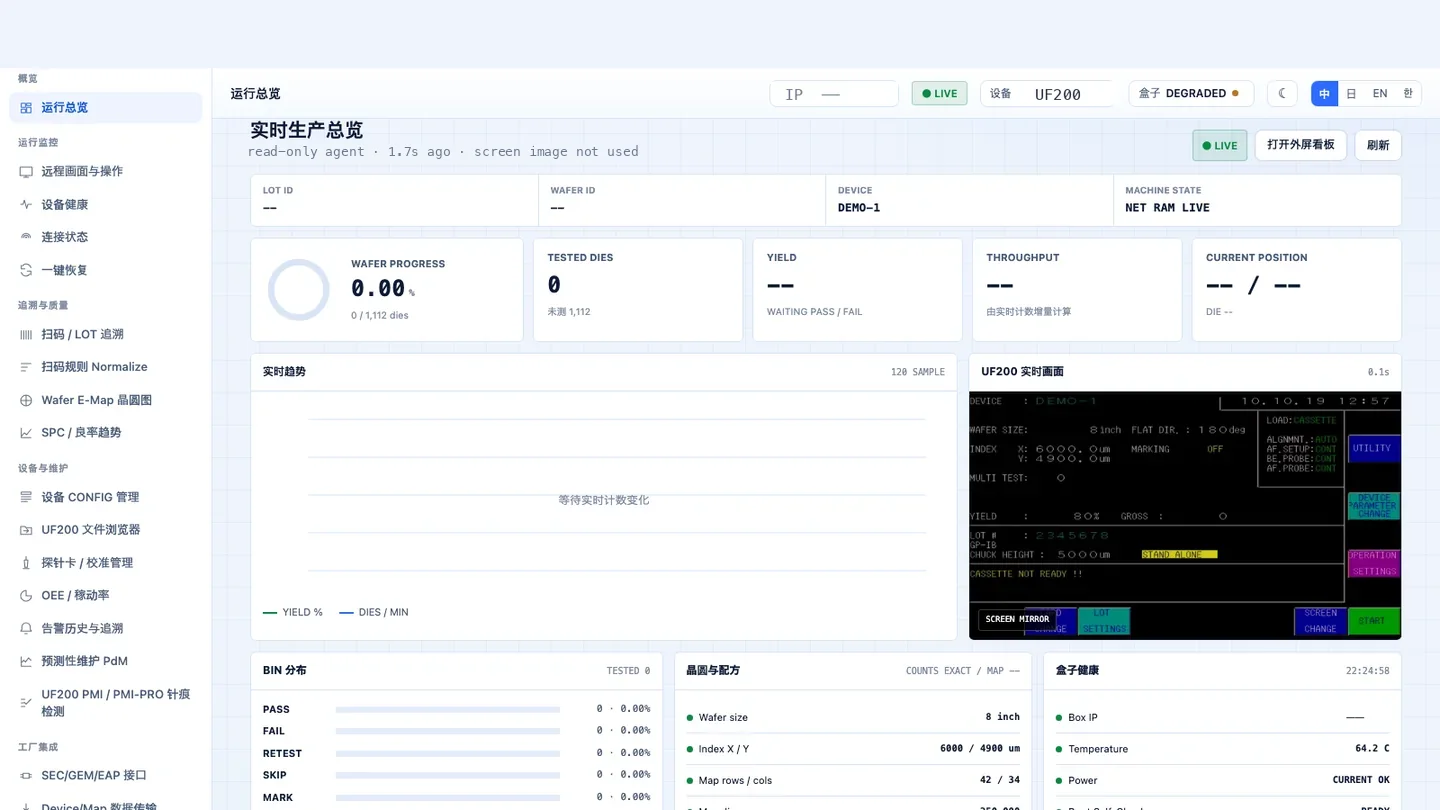
This board shows the information box's live overview page: LOT / WAFER / DEVICE and machine state, wafer progress and tested dies, bin distribution, wafer and recipe, box health, and the machine's live screen alongside. Every number comes from the machine's own counters and configuration; anything not read shows as -- rather than being estimated or filled in. Engineering prototype: the screen comes from our own engineering machine, and there are no customer deliveries yet.
A real screen from our engineering machine; internal identifiers (addresses, device ids, component names) are painted out.
Prober Information Box
A bolt-on unit that leaves the prober untouched and reads wafer geometry, test counters and probe-card counts from the machine itself. Engineering prototype.
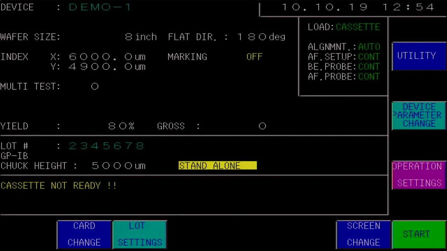
The prober's native screen is mirrored read-only to the browser and to this board: DEVICE, wafer size and flat direction, index X/Y, yield and gross, LOT number, chuck height, and the machine's own alarm lines, all shown as they are — not rewritten, not tidied up. Remote operation is an option; read-only is the default. Engineering prototype, with no customer deliveries yet.
A real screen from our engineering machine; internal identifiers (addresses, device ids, component names) are painted out.
Prober Information Box
A bolt-on unit that leaves the prober untouched and reads wafer geometry, test counters and probe-card counts from the machine itself. Engineering prototype.
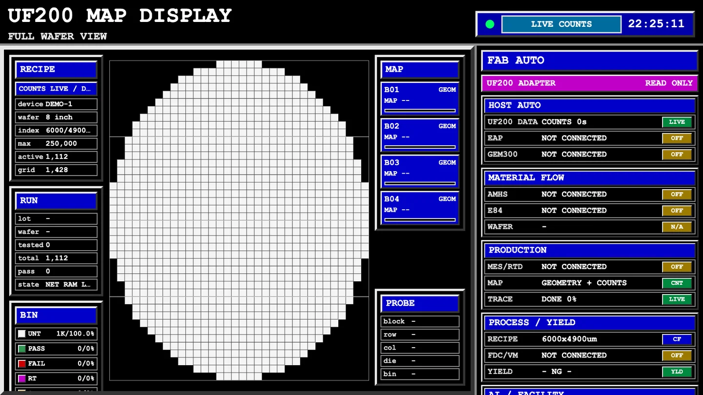
The whole die map and every link state on one screen
The external large-screen view: recipe, run and bin counts down the left, the full wafer die map rebuilt from index X/Y and the grid size in the middle, and the state of every link — fab automation, host automation, material flow, production and yield — down the right. A link that is not connected reads NOT CONNECTED, and the adapter side is marked READ ONLY: nothing is shown as online just to make the board look better. Engineering prototype, with no customer deliveries yet.
A real screen from our engineering machine; internal identifiers (addresses, device ids, component names) are painted out.
Prober Information Box
A bolt-on unit that leaves the prober untouched and reads wafer geometry, test counters and probe-card counts from the machine itself. Engineering prototype.
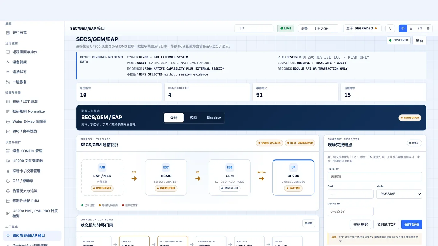
17 · Production board · SECS/GEM and EAP interface
Evidence first; where there is none, it says so
This page verifies the machine's native GEM/HSMS programs, data dictionary and runtime logs directly, and keeps the external host configuration separate from the current session state: on the protocol topology, EAP/MES, HSMS, GEM and the machine side each carry their own mark — evidence held, inference pending, or blocked. Where there is no evidence, no verdict is issued. AMHS, E84 and AGV/OHT interlocks are interfacing capabilities of the upgrade package; this workshop does not itself run an overhead transport. Engineering prototype, with no customer deliveries yet.
A real screen from our engineering machine; internal identifiers (addresses, device ids, component names) are painted out.
Prober Information Box
A bolt-on unit that leaves the prober untouched and reads wafer geometry, test counters and probe-card counts from the machine itself. Engineering prototype.
This page describes refurbishment, retrofit and delivery services for pre-owned equipment. Maker model names indicate the machines we can work on; they do not imply authorisation, certification or endorsement by those makers. Retrofits and rebuilds are carried out by us, under our own responsibility. The hall is an illustrative scene built from the real machines and real screens; the overhead transport stands for the AMHS material flow the upgrade package can interface with, and is not equipment of this workshop. The barcode scanner is under improvement and the information box and its four board screens are an engineering prototype — both are our own projects with no customer deliveries yet, and the page says so station by station.
Tell us the model and we will quote it
A digital twin of a CP bay modelled on the actual machines: six probers along the north side - TSK APM90A, UF200, UF3000, UF3000ex, AP3000 and the TEL P-12XL - and four test cells facing them: docking cells for the Advantest V93000, the Advantest T5833 and the Teradyne M5, plus a cable-connected Advantest EVA100. The four production boards on the wall are real screens from our own information box. Click any machine or board and the detail appears below.