
Image sensor test · solution stage
CMOS Image Sensor Test Solution
The bottleneck in image sensor test is not the test list, it is the image data: once frames get large and sites multiply, shipping every frame back to a workstation eats the takt. This solution puts the compute at the site - one APU image board per site on the EVA100 platform, capture over MIPI CSI-2 or DVP, and the algorithm executed locally, so sites stay independent of one another.
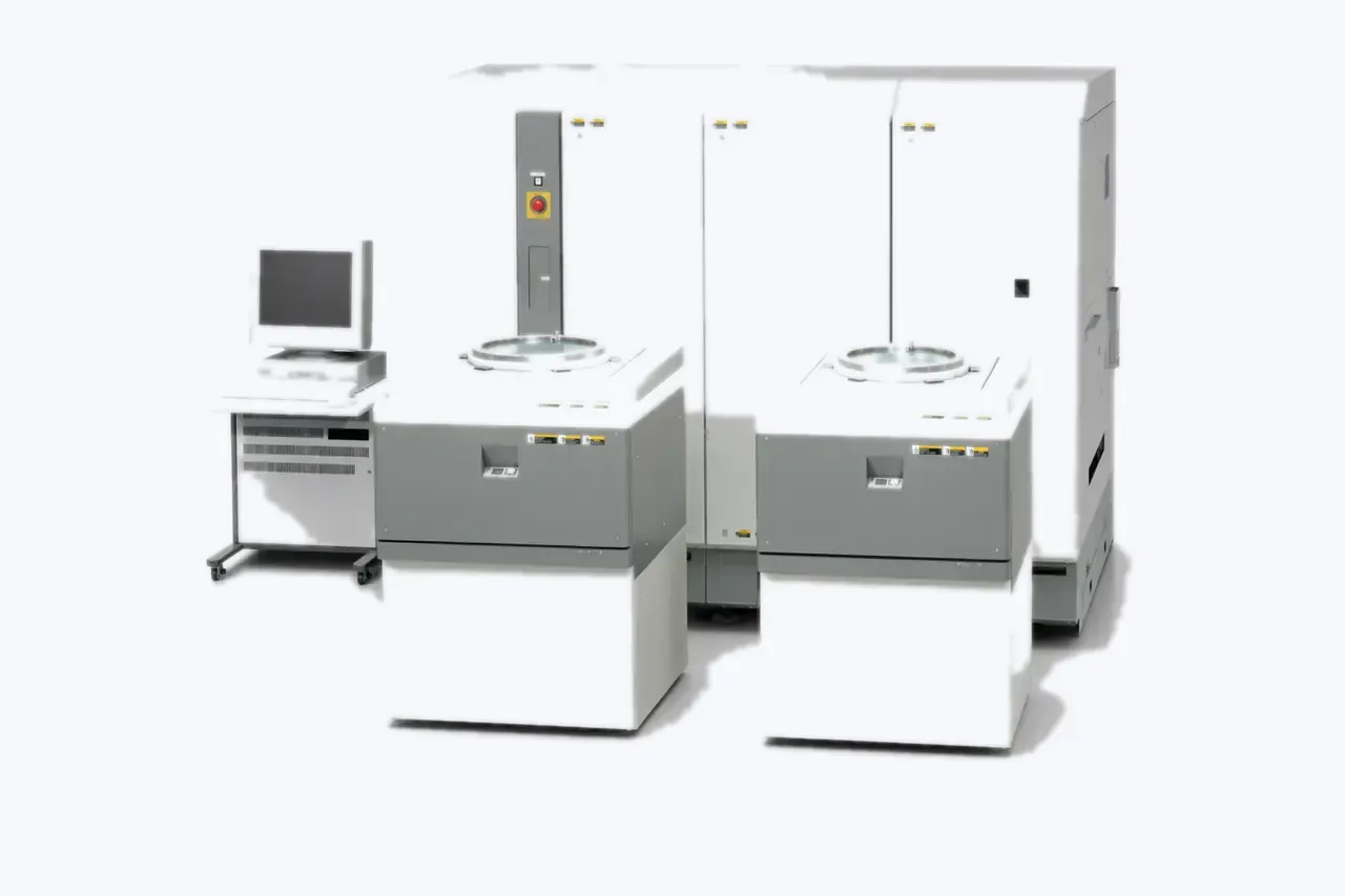
Category visual, not an actual EVA100. The solution hardware form follows the actual engineering definition.
The same points in words
- Stage
- Not a product for sale
- Architecture
- Capture and processing stay local to the site
- Interface
- DVP 10/12-bit and LVDS as possible extensions
- Compute
- Quad Arm cores + 128 GPU cores
Equipment and engineering solution
Applications
The solution covers the following application areas.
Multi-site parallel CIS testing
Image-interface capture
Local algorithm execution
The same points in words
- Multi-site parallel CIS testing
- Each site processes its own image data, avoiding the communication cost of centralized upload - especially suited to trim-style operations.
- Image-interface capture
- Capture over MIPI CSI-2 D-PHY with 1/2/4 data lanes; DVP 10/12-bit and LVDS are possible extensions, covering the RGB, YUV and RAW format families.
- Local algorithm execution
- Under demo conditions, algorithms on 3264 x 2464 images across 8 frames run in about 100 ms.
SPECIFICATIONS
Specifications
The final configuration follows the device interface, image format, site count and engineering conditions.
See the full specification table
| Item | Specification / configuration | Notes |
|---|---|---|
| Image formats | RGB888/666/565; YUV422-8b/444-8b; RAW6/7/8/10/12/14 | Configured to the device output format |
| Software stack | EVA test sequences / image-processing API / light-source API / APU driver | Runs on the EVA100 system software |
| Demo result | 3264 x 2464, 8 frames, algorithm time approx. 100 ms | Demo conditions as stated in the training document |
| Route direction | D-PHY toward 2.5 Gbps/lane; C-PHY toward 2.5 Gsym/s per trio | The documented roadmap dates are from 2021; current status requires engineering confirmation |
WORKFLOW
Workflow
01 Device and interface confirmation
02 APU and light-source configuration
03 Algorithm and sequence development
04 Solution validation
The same points in words
- Device and interface confirmation
- Typical flow once a project starts: confirm the sensor output interface, image format and site count.
- APU and light-source configuration
- Configure image boards, the controlled light source and EVA100 resources per site count.
- Algorithm and sequence development
- Image-processing algorithms deploy on the APU; test sequences run on the EVA100.
- Solution validation
- Validate takt and data path with demos and samples, then define the delivery form.
PROJECT OUTLINE
Prospective project delivery
Requirement and device evaluation
Technical agreement
Solution validation
Delivery definition
The same points in words
- Requirement and device evaluation
- Confirm the sensor interface, image format, site count and target takt.
- Technical agreement
- Define the solution scope, hardware composition, algorithm boundary and responsibilities.
- Solution validation
- Validate the data path and takt with samples and demos.
- Delivery definition
- Define the delivery form and acceptance based on validation results.
CONFIGURATION
Configuration and acceptance
The sections below describe the solution's sources, ownership boundary and undefined items.
Source and stage
Content comes from the CMOS image sensor solution chapter of a 2022 EVA100 training document (system architecture, APU specification and demo data); the documented roadmap dates are from 2021, so this page presents a technology route, with no claim of a product for sale.
Ownership boundary
The solution is built on the Advantest EVA100 platform; the engineering owner of the image board (APU) is not stated in the source, so this page makes no in-house-development claim.
Undefined items
The test-item list, judgment methods and delivery form are not defined in the source and must be established per engineering project.
Share the device interface, image format and target
Send the sample, installed equipment, current issue and target takt. We will acknowledge receipt within one business day.