DeepTouch1000

Products and engineering

Assembly, test, cleaning and storage

Browse by probe card process, or open the specifications for PCT5801, DeepTouch1000, the high-pin-count socket tester and EVA100.

01 / ASSEMBLY

MEMS probe card assembly

Build the station around the probe, substrate, fixture, vision alignment, recipes and post-assembly validation.

Configuration: probe type, substrate, datum, accuracy, takt and acceptance method.

Fixture and changeover

Design holding, datum and changeover for the probe, substrate and assembly process.

Vision-assisted alignment

Confirm placement and retain process and exception images.

Recipe and traceability

Record work order, material, operator, recipe version and result.

Post-assembly validation

Connect AOI, XYZ, Pin Force and electrical checks.

02 / ELECTRICAL + PHYSICAL TEST

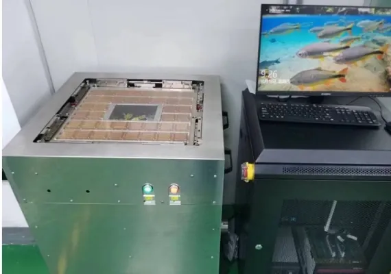
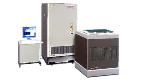
PCT5801 and DeepTouch1000

PCT5801 handles high-channel electrical tests; DeepTouch1000 checks load, probe-tip XYZ and contact state.

Current configuration: 16,384 channels and 0-1000 kgf. 60k/300k HBM systems are designed for the target card and interfaces.

Open / Short / Leakage

Continuity, short and nA-level leakage. A typical 10k-pin / 10 nA Leakage task is about 60 minutes.

Control resources

MCW, Relay, FPGA, ASIC, SPI and I²C checks.

High-channel expansion

1,024-channel modules are combined for the motherboard and tester.

Physical validation

Load, probe-tip XYZ, probe marks and contact state support electrical anomaly analysis.

03 / CLEAN + REINSPECT

Probe card cleaning and reinspection

Manage atomized IPA, controlled brushing, clean gas and three-direction image review by recipe.

Configuration: probe type, material compatibility, particle limits, rework conditions and task time.

Atomized IPA

Set delivery range and process parameters for the card.

Controlled brushing

Manage brush type, movement, contact and cycle count.

Clean-gas blowoff

Establish a stable state for reinspection and electrical test.

Three-direction review

Retain images, judgement and rework history.

04 / CONTROLLED STORAGE

Traceable probe card storage

Manage receipt, issue, return and inventory through environment control, RFID and factory-system interfaces.

Configuration: capacity, environment, RFID, WMS/EAP/MES, handoff method and store/retrieve time.

Controlled environment

Set nitrogen, ESD, temperature/humidity and alarms for the card and facility.

RFID identity

Link card ID, location, state and movement history.

WMS / EAP / MES

Receive tasks and return state, exception and audit records.

Manual or automated handoff

Configure manual, AMR, robot or OHT handling.

OTHER EQUIPMENT AND SERVICES

Sockets, EVA100 and surplus equipment

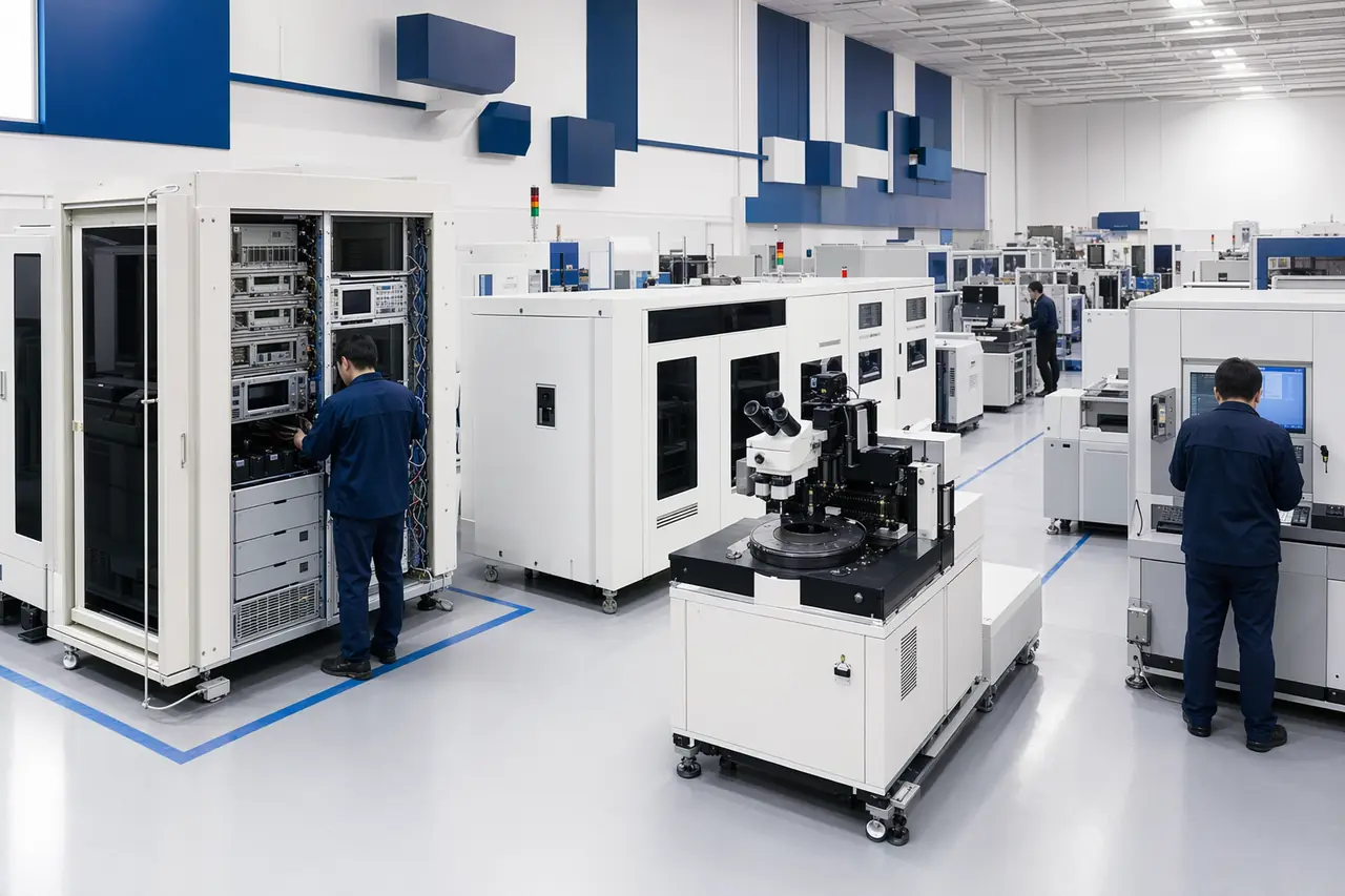
High-pin-count socket testers, EVA100 test-program development and surplus semiconductor equipment are listed here.

High-pin-count AI processor socket test equipment

High-Pin-Count AI Processor Socket Tester

Contact and electrical validation for 8,000-20,000-pin AI processor sockets before expensive processor and system assembly.

View full details
Advantest EVA100 test equipment

Advantest EVA100 Application and Test Engineering

Application engineering for EVA100 across logic, PMIC, comparator, amplifier, converter and sensor testing, including CP/FT, IP validation and failure analysis.

View full details
Portfolio illustration of surplus lithography, prober and test equipment

Surplus Semiconductor Equipment and Engineering

Scope covering ASML lithography, Accretech/TEL probers and Advantest ATE, with inventory, configuration, logistics and installation confirmed per unit.

View full details
EQUIPMENT INFORMATION

Nine equipment pages

Each page lists applications, specifications, operating steps, project delivery and acceptance conditions.

High-channel electrical and physical validationMemory Probe Card Test SystemA probe card validation platform for HBM and high-pin-count applications, combining Open, Short, nA-level leakage, control resources and physical inspection.Modular high-channel electrical inspectionPCT5801 Probe Card Electrical Test PlatformA modular probe card electrical test platform for Open, Short, nA-level Leakage, control resources and optional AC/TDR paths.Load, probe-tip XYZ and contact evidenceDeepTouch1000 Probe Card Physical ValidationA 0-1000 kgf load-engineering and probe-tip XYZ inspection platform that can correlate physical evidence with PCT5801 electrical results.Fixture, vision alignment, recipe and post-assembly validationMEMS Probe Card Pin-Assembly EquipmentAn equipment route around probes, substrate, fixtures, vision-assisted alignment, recipe traceability and post-assembly AOI/XYZ/Pin Force/electrical checks.Atomized IPA, controlled brushing, clean gas and closed-loop reviewProbe Card Cleaning and Three-Direction ReinspectionControlled probe card cleaning with atomized IPA, controlled brushing, clean-gas blowoff, three-direction image review and RFID traceability.Controlled environment, RFID and factory interfacesTraceable Probe Card Storage SystemControlled probe card storage with nitrogen/ESD, RFID, WMS/EAP/MES interfaces and manual, AMR, robot or OHT handoff.Contact and electrical validation before system assemblyHigh-Pin-Count AI Processor Socket TesterContact and electrical validation for 8,000-20,000-pin AI processor sockets before expensive processor and system assembly.Digital, mixed-signal and application-development workflowAdvantest EVA100 Application and Test EngineeringApplication engineering for EVA100 across logic, PMIC, comparator, amplifier, converter and sensor testing, including CP/FT, IP validation and failure analysis.Equipment scope, condition review and project deliverySurplus Semiconductor Equipment and EngineeringScope covering ASML lithography, Accretech/TEL probers and Advantest ATE, with inventory, configuration, logistics and installation confirmed per unit.