
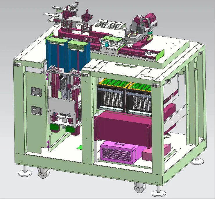
In development · design stage
ECP1010 Embedded-Chip PCB Automatic Test System
Once the IC is embedded inside the PCB, the only accessible test points are the pads on the board surface; production lines currently use ICT for open/short, leakage and specified LRC checks, which cannot cover device-level functional test. ECP1010 is Probing's in-development automatic test system for embedded-chip PCB: batch substrates load and unload automatically, vision alignment and press-down contact establish the connection, and a built-in ATE measures 1,024 channels directly, expanded to 16,384 through a relay matrix, running parametric and functional tests on the embedded digital and analog chips. The product is at the design and engineering stage; this page follows the design documentation.
Design rendering from the brochure, not a photo of a built machine. Structure and configuration follow the final delivery.
The same points in words
- Stage
- Specifications follow the technical agreement
- Test object
- Electrical test of digital and analog chips
- Channels
- Relay-matrix expansion to 16,384
- Automation
- 2D-code reading and laser marking
Equipment and engineering solution
Applications
Designed for the following embedded-chip PCB substrate test tasks.
Embedded-chip substrate electrical test
Process validation and fault isolation
Traceability and marking
The same points in words
- Embedded-chip substrate electrical test
- Run batch parametric and functional tests on PCB substrates with embedded digital and analog chips.
- Process validation and fault isolation
- Use ATE-grade board resources for device parameters and function items, and trace failures to the specific substrate.
- Traceability and marking
- Link results through 2D-code identification and finish with automatic laser marking.
SPECIFICATIONS
Specifications
The final configuration follows the substrate, interfaces, site conditions and acceptance items.
See the full specification table
| Item | Specification / configuration | Notes |
|---|---|---|
| Vision and marking | One CCD set with 2D-code reading | Automatic laser-marking unit (added in the 2024-07 proposal) |
| Built-in ATE · digital | 1,024 channels, 200 MHz, 128 M vector depth | Digital driver/comparator boards: −1.25 to +7 V, ±32 mA, 18-bit waveform generation and capture |
| Built-in ATE · analog and HV | Analog, medium-power and high-voltage source-measure configured per test item | Module specifications are provided in the technical agreement |
| Built-in ATE · waveform | LF 24-bit: 200 ksps AWG / 625 ksps DGT; HF 16-bit: 512 Msps AWG / 250 Msps DGT | Oscilloscope board 1 Gsps, 500 MHz, 8,000 sample points |
| Protocols | I2C, SPI, JTAG and arbitrary protocols | Configured per device specification |
| Software | Graphical sequence programming, vector edit and debug, logic analysis, virtual instruments, Shmoo, VI-curve reports, STILReader, CATVert-VCD | Production control panel, GPIB driver editor, real-time result reports |
| Facilities (proposal figures) | AC 380 V three-phase 50 Hz, approx. 8 kW | Approx. 1550 x 1400 x 1700 mm, approx. 1200 kg |
| Design iteration direction | 2024-07 proposal: substrate range 45 x 50 to 95 x 240 mm, thickness 0.1-2 mm; alignment accuracy ±5 μm (single side); minimum pad 0.15 mm at 0.2 mm pitch | Coexists with the brochure figures; the technical agreement decides the final values |
WORKFLOW
Workflow
01 Stack loading and interleaf removal
02 Vision alignment and press-down
03 ATE electrical test
04 Marking and unloading
The same points in words
- Stack loading and interleaf removal
- Batch substrates separate automatically; interleaving paper is removed on loading.
- Vision alignment and press-down
- CCD alignment followed by press-down contact establishes the test connection.
- ATE electrical test
- Digital and analog board resources run the parametric and functional test items.
- Marking and unloading
- Results link to the 2D code; after laser marking, substrates unload with interleaving paper re-inserted.
FAT / SAT
Project delivery
Sample evaluation
Technical agreement
FAT
SAT
The same points in words
- Sample evaluation
- Confirm the object, interfaces, current state, failure modes and available validation samples.
- Technical agreement
- Define configuration, measurement method, limits, takt, data interfaces and responsibilities.
- FAT
- Verify functions, repeatability, reporting and exception handling with agreed samples.
- SAT
- Complete site integration, training, upstream/downstream interfaces and issue closure.
CONFIGURATION
Configuration and acceptance
System configuration, optional items and acceptance conditions are summarized below.
Stage discipline
Four design documents from 2023-06 to 2024-07 show the specification still iterating, with no delivery or acceptance records; this page presents ECP1010 as an in-development machine and its image as a design rendering.
Parameter sources
Specifications follow the 2023-06 public brochure; the 2024-07 proposal's substrate range, alignment accuracy and laser marking are listed separately as the design iteration direction, with the differences across proposal revisions stated on this page.
Boundary
Built-in ATE board resources are as stated in the design documentation; test items, limits and the final configuration are defined in the technical agreement.
Share the substrate, interfaces and target
Send the sample, installed equipment, current issue and target takt. We will acknowledge receipt within one business day.