From needle cutting to storage: which tools on this chain are ours

The cost of a probe card rarely stops at purchase: assembly consistency, post-clean residue, storage environment, test criteria — wherever a line lacks the equipment for one of these, the problem surfaces later, in volume production. This MEMS probe-card manufacturing and validation cleanroom lays out the whole chain by its real process bays and marks which parts our equipment covers and which are left to specialist suppliers. Click any tool to zoom in on what it does and the product behind it; the two ends of the room are incoming and shipping.

4 Production · 4 Engineering · 1 Development

Drag to orbit · scroll to zoom · click a tool to zoom in

What this workshop is made of, and what it can do

Stations14
We supply4
Flagship pin count300,000
Whole-card force1000 kgf
  1. incoming
  2. assembly
  3. test
  4. clean
  5. storage
  6. ship
The same points in words
What this workshop is made of, and what it can do
Fourteen stations run from incoming stock to shipment. Four of them we supply in production, four are in engineering, one is in development, and the remaining five are steps any such workshop already has.

How the work runs

  1. Card type and the problem
  2. Method and jigs defined
  3. We build the machine
  4. Installed and signed off
  5. We stay with it in production

Drag to orbit, scroll to zoom. Click any tool to fly in and read what it does.

Not supplied

01 · Probe Incoming Inspection and Sorting

Measure and bin probes

Released probes are measured for length, tip form and straightness, then binned and loaded into carrier trays for the assembly line to draw from.

How it works

  1. stock in
  2. check
  3. sort
  4. release
The same points in words
Probe Incoming Inspection and Sorting
Probing does not supply equipment for this step.
Not supplied

02 · Guide Plate Machining (Vertical Probe Cards)

Machine guide-hole array

Upper and lower guide plates are laser-drilled or EDM-machined with the guide-hole array that constrains each vertical probe and sets its buckling geometry; Probing does not supply equipment for this step.

How it works

  1. datum
  2. drill
  3. verify
  4. handover
Not supplied

03 · PCB / ST Incoming Flying-Probe Test

Electrical check before assembly

Purchased probe card PCBs and space transformers are spot-checked for continuity and resistance on a double-sided flying-probe tester before entering assembly; this equipment is outside Probing's scope of supply.

How it works

  1. board in
  2. probe path
  3. open/short
  4. report
Engineering

04 · Laser probe cutting

Cut to length and drop to tray

Probe stock is fed in as wire or as an array, a laser cuts each probe to the target length, and the cut probe drops into the tray for pickup.

Process chainPick → align → weld
JoiningLaser micro-welding
Post-weld checkAutofocus inspection
Closed loopPCT5801 + DeepTouch1000

How it works

  1. feed
  2. cut
  3. to length
  4. to tray

MEMS Probe Card Pin Assembly and Laser Micro-Welding

Full specification and process

Specifications

ScopeMEMS and project-defined probe / substrate combinationsProbe type, material and datum confirmed on samples
Pick stationProbe taken from the tray and presented to the alignment stageSlot-to-probe clearance designed per probe type
Alignment stationAlignment stage corrects attitude and positionCoplanarity of fixed and moving jaws drives handover distortion
Weld stationWeld gripper transfers the probe for laser micro-weldingEnergy and dwell time held in the recipe
Gripper requirementFixed and moving jaw, pneumatic actuationClearance matched to probe thickness: too wide loses grip, too tight deforms the probe
Post-weld inspectionAutofocus check of weld positionAlso the reference contact point for wafer electrical test
Recipe and traceabilityWork order, material, operator, recipe version and resultSupports version traceability and review
Post-assembly validationAOI, probe-tip XYZ, Pin Force and electrical checksCombination selected by acceptance method
SafetyMotion limits, fixture interlock and fault stopConfirmed by equipment risk assessment

Evidence and record

Process parametersPlacement accuracy and UPH are determined by sample trials on the target probe, substrate and fixture; no universal cross-customer figure is published.
Closed-loop capabilityPCT5801 covers post-weld electrical verification and DeepTouch1000 covers whole-card touchdown and 3D tip inspection, so anomalies trace back to a specific probe position.
DeliverablesFixtures, algorithms, takt and the post-inspection combination are written into the technical agreement and verified at FAT/SAT.
Open the equipment page →
The same points in words
Laser probe cutting
The drawing shows a generic industry configuration, not a measured mechanism of a specific machine.
Process chain
Three gripper handovers
Joining
Joint condition confirmed by vision
Post-weld check
Confirms weld position and contact face
Closed loop
Electrical and whole-card mechanical re-verification
New card introduction
Establish process windows and fixture design from probe type, substrate and datum.
Manual-process standardization
Turn operator-dependent steps into recipes, images, judgements and exception records.
Post-assembly quality loop
Relate AOI, XYZ, probe height/force and electrical results to the assembly lot.
Pick
The pick gripper takes the probe from the tray and seats it against the alignment datum Avoiding added distortion during handover is the precondition for accuracy
Align
The alignment stage clamps and corrects probe attitude Gripper coplanarity and perpendicularity are the critical assembly metrics
Weld
The weld gripper transfers the probe and laser micro-welding runs Joint consistency controlled by vision and recipe
Verify
Autofocus position check, then PCT5801 and DeepTouch1000 Locates weld problems while still at the assembly stage
Engineering

05 · Probe Pick and Alignment

Pick and align the probe

The pick gripper takes each probe from the tray and seats it against the fixed jaw of the alignment stage, which clamps it and corrects attitude and position, with jaw clearance matched to probe thickness.

Process chainPick → align → weld
JoiningLaser micro-welding
Post-weld checkAutofocus inspection
Closed loopPCT5801 + DeepTouch1000

How it works

  1. pick
  2. straighten
  3. hand over
  4. place

MEMS Probe Card Pin Assembly and Laser Micro-Welding

Full specification and process

Specifications

ScopeMEMS and project-defined probe / substrate combinationsProbe type, material and datum confirmed on samples
Pick stationProbe taken from the tray and presented to the alignment stageSlot-to-probe clearance designed per probe type
Alignment stationAlignment stage corrects attitude and positionCoplanarity of fixed and moving jaws drives handover distortion
Weld stationWeld gripper transfers the probe for laser micro-weldingEnergy and dwell time held in the recipe
Gripper requirementFixed and moving jaw, pneumatic actuationClearance matched to probe thickness: too wide loses grip, too tight deforms the probe
Post-weld inspectionAutofocus check of weld positionAlso the reference contact point for wafer electrical test
Recipe and traceabilityWork order, material, operator, recipe version and resultSupports version traceability and review
Post-assembly validationAOI, probe-tip XYZ, Pin Force and electrical checksCombination selected by acceptance method
SafetyMotion limits, fixture interlock and fault stopConfirmed by equipment risk assessment

Evidence and record

Process parametersPlacement accuracy and UPH are determined by sample trials on the target probe, substrate and fixture; no universal cross-customer figure is published.
Closed-loop capabilityPCT5801 covers post-weld electrical verification and DeepTouch1000 covers whole-card touchdown and 3D tip inspection, so anomalies trace back to a specific probe position.
DeliverablesFixtures, algorithms, takt and the post-inspection combination are written into the technical agreement and verified at FAT/SAT.
Open the equipment page →
The same points in words
Process chain
Three gripper handovers
Joining
Joint condition confirmed by vision
Post-weld check
Confirms weld position and contact face
Closed loop
Electrical and whole-card mechanical re-verification
New card introduction
Establish process windows and fixture design from probe type, substrate and datum.
Manual-process standardization
Turn operator-dependent steps into recipes, images, judgements and exception records.
Post-assembly quality loop
Relate AOI, XYZ, probe height/force and electrical results to the assembly lot.
Pick
The pick gripper takes the probe from the tray and seats it against the alignment datum Avoiding added distortion during handover is the precondition for accuracy
Align
The alignment stage clamps and corrects probe attitude Gripper coplanarity and perpendicularity are the critical assembly metrics
Weld
The weld gripper transfers the probe and laser micro-welding runs Joint consistency controlled by vision and recipe
Verify
Autofocus position check, then PCT5801 and DeepTouch1000 Locates weld problems while still at the assembly stage
Engineering

06 · Laser Micro-Welding Pin Attach

Bond consistency held by recipe, not by feel

The weld gripper takes the aligned probe from the stage, places it on its substrate pad and runs the laser micro-weld, with joint energy and dwell time held in the recipe.

Process chainPick → align → weld
JoiningLaser micro-welding
Post-weld checkAutofocus inspection
Closed loopPCT5801 + DeepTouch1000

How it works

  1. align
  2. laser weld
  3. vision check
  4. to recipe

What we take on

  • New card introduction
  • Manual-process standardization
  • Post-assembly quality loop
  1. 01Pick
  2. 02Align
  3. 03Weld
  4. 04Verify

MEMS Probe Card Pin Assembly and Laser Micro-Welding

Full specification and process

Specifications

ScopeMEMS and project-defined probe / substrate combinationsProbe type, material and datum confirmed on samples
Pick stationProbe taken from the tray and presented to the alignment stageSlot-to-probe clearance designed per probe type
Alignment stationAlignment stage corrects attitude and positionCoplanarity of fixed and moving jaws drives handover distortion
Weld stationWeld gripper transfers the probe for laser micro-weldingEnergy and dwell time held in the recipe
Gripper requirementFixed and moving jaw, pneumatic actuationClearance matched to probe thickness: too wide loses grip, too tight deforms the probe
Post-weld inspectionAutofocus check of weld positionAlso the reference contact point for wafer electrical test
Recipe and traceabilityWork order, material, operator, recipe version and resultSupports version traceability and review
Post-assembly validationAOI, probe-tip XYZ, Pin Force and electrical checksCombination selected by acceptance method
SafetyMotion limits, fixture interlock and fault stopConfirmed by equipment risk assessment

Evidence and record

Process parametersPlacement accuracy and UPH are determined by sample trials on the target probe, substrate and fixture; no universal cross-customer figure is published.
Closed-loop capabilityPCT5801 covers post-weld electrical verification and DeepTouch1000 covers whole-card touchdown and 3D tip inspection, so anomalies trace back to a specific probe position.
DeliverablesFixtures, algorithms, takt and the post-inspection combination are written into the technical agreement and verified at FAT/SAT.
Open the equipment page →
The same points in words
Process chain
Three gripper handovers
Joining
Joint condition confirmed by vision
Post-weld check
Confirms weld position and contact face
Closed loop
Electrical and whole-card mechanical re-verification
New card introduction
Establish process windows and fixture design from probe type, substrate and datum.
Manual-process standardization
Turn operator-dependent steps into recipes, images, judgements and exception records.
Post-assembly quality loop
Relate AOI, XYZ, probe height/force and electrical results to the assembly lot.
Pick
The pick gripper takes the probe from the tray and seats it against the alignment datum Avoiding added distortion during handover is the precondition for accuracy
Align
The alignment stage clamps and corrects probe attitude Gripper coplanarity and perpendicularity are the critical assembly metrics
Weld
The weld gripper transfers the probe and laser micro-welding runs Joint consistency controlled by vision and recipe
Verify
Autofocus position check, then PCT5801 and DeepTouch1000 Locates weld problems while still at the assembly stage
Engineering

07 · Post-Weld Autofocus Inspection

Bond defects found here, not in volume

An autofocus vision unit confirms the weld position and contact face of each finished joint, and the result is written to the work order with material, operator and recipe version, and serves as the contact-position reference for wafer electrical test.

Process chainPick → align → weld
JoiningLaser micro-welding
Post-weld checkAutofocus inspection
Closed loopPCT5801 + DeepTouch1000

How it works

  1. autofocus
  2. position
  3. flag it
  4. to the batch

MEMS Probe Card Pin Assembly and Laser Micro-Welding

Full specification and process

Specifications

ScopeMEMS and project-defined probe / substrate combinationsProbe type, material and datum confirmed on samples
Pick stationProbe taken from the tray and presented to the alignment stageSlot-to-probe clearance designed per probe type
Alignment stationAlignment stage corrects attitude and positionCoplanarity of fixed and moving jaws drives handover distortion
Weld stationWeld gripper transfers the probe for laser micro-weldingEnergy and dwell time held in the recipe
Gripper requirementFixed and moving jaw, pneumatic actuationClearance matched to probe thickness: too wide loses grip, too tight deforms the probe
Post-weld inspectionAutofocus check of weld positionAlso the reference contact point for wafer electrical test
Recipe and traceabilityWork order, material, operator, recipe version and resultSupports version traceability and review
Post-assembly validationAOI, probe-tip XYZ, Pin Force and electrical checksCombination selected by acceptance method
SafetyMotion limits, fixture interlock and fault stopConfirmed by equipment risk assessment

Evidence and record

Process parametersPlacement accuracy and UPH are determined by sample trials on the target probe, substrate and fixture; no universal cross-customer figure is published.
Closed-loop capabilityPCT5801 covers post-weld electrical verification and DeepTouch1000 covers whole-card touchdown and 3D tip inspection, so anomalies trace back to a specific probe position.
DeliverablesFixtures, algorithms, takt and the post-inspection combination are written into the technical agreement and verified at FAT/SAT.
Open the equipment page →
The same points in words
Process chain
Three gripper handovers
Joining
Joint condition confirmed by vision
Post-weld check
Confirms weld position and contact face
Closed loop
Electrical and whole-card mechanical re-verification
New card introduction
Establish process windows and fixture design from probe type, substrate and datum.
Manual-process standardization
Turn operator-dependent steps into recipes, images, judgements and exception records.
Post-assembly quality loop
Relate AOI, XYZ, probe height/force and electrical results to the assembly lot.
Pick
The pick gripper takes the probe from the tray and seats it against the alignment datum Avoiding added distortion during handover is the precondition for accuracy
Align
The alignment stage clamps and corrects probe attitude Gripper coplanarity and perpendicularity are the critical assembly metrics
Weld
The weld gripper transfers the probe and laser micro-welding runs Joint consistency controlled by vision and recipe
Verify
Autofocus position check, then PCT5801 and DeepTouch1000 Locates weld problems while still at the assembly stage
Production

08 · Probe Tip XYZ and Planarity Metrology

Which pins are out of tolerance, answered by coordinate

The populated card is scanned probe by probe for tip X, Y and Z position, probe length and array planarity, and positions outside the project threshold are flagged by coordinate.

Chuck force1000 kgf
Maximum pins300,000
StructurePB5801 all-in-one
Geometry3D probe-tip XYZ scan

How it works

  1. card in
  2. tip XYZ
  3. planarity
  4. data out

What we take on

  • High-pin-count card loading
  • Tip position and consistency
  • Electrical anomaly review
  • Incoming probe-card verification
  1. 01Confirm card and fixture
  2. 02Load and image
  3. 03Analyze XYZ and load
  4. 04Correlate electrical results

DeepTouch1000 Probe Station for Probe Card Test

Full specification and process

Specifications

Chuck force1000 kgf (about 9.81 kN)Whole-card validation of a high-pin-count card needs more than 450 kgf
Maximum pins300,000Configured for the target card and motherboard
StructurePB5801 all-in-oneProbe station integrated with the probe card test system
Load portMedia Loader PortCarrier in/out and sorting through the loader port
Force displayChuckForce DisplayLive chuck-force readout during touchdown
Device handlingHBM handlingHandling and alignment for high-stack devices
Tip inspection3D probe-tip XYZTip length, position deviation and planarity scanning
TemperatureTri-temperature (option)Range set by configuration and test conditions
POST unit (option)PinForce measurement and contact checkPressure sensor resolution 2 g, full scale 200 g, probe positioning accuracy 0.3 μm
Main body dimensions1320 × 1930 × 1500 mmNominal dimensions from specification RevA1
VibrationHigh-performance isolation platformSuppresses external vibration during tip measurement
Motion controlXY control resolution 40 nm; Z accuracy ±2 µm with 0.1 µm control resolutionSpecification RevA1
Tip imaging resolutionX/Y 0.345 µm; Z 0.5 µmThree-dimensional probe tip inspection optics
Card compatibilityVertical, cantilever and MEMS probe cardsAccepts 4.5 / 9 / 12 inch cards
Card alignment rangeX ±164 mm; Y 160 mm front, 130 mm rear3D imaging range 80 mm to the rear
Wafer300 mmAutomatic probe card exchange cart is optional
Temperature systemChuck surface −55 °C to 200 °C (system range −55 to +180 °C)Electric heating with CDA cooling; RevA1 specification, configuration lists differ - confirmed per project
XY/theta travel and accuracyXY accuracy +/-2 um; X +/-163 mm, Y +280 / -165 mm; up to 600 mm/sRevA1 specification
Z travel and contact window81.5 mm travel; contact set between 59.2 and 79.0 mm; up to 5 mm/s; +/-2 um overshootSetting window under the full 1000 kgf load
Chuck flatness15 um between 20 and 50 °C; 30 um between 50 and 200 °CBanded by temperature - the critical figure for full-card touchdown
Chuck electricalLeakage < 20 pA at 25 °C/10 V, < 30 pA at 200 °C/10 V; test voltage to 500 V300 mm chuck assembly figures, confirmed with the temperature option
Mass and site conditions2,000 kg; 25 °C +/-3 °C, humidity <= 65 %; floor vibration frequency >= 10 Hz recommendedInstallation conditions to check when choosing a site
UtilitiesSingle-phase AC 200/220/230/240 V three-wire, 50/60 Hz; 20 ms ride-through; 2.3 kVARevA1 specification
Standard softwareLive wafer map (PASS/FAIL/BIN, two-colour or multi-colour), manual inspection, offline recipe editing, log and result exportStandard configuration
Operator interfaceColour LCD 1920 x 1080, Chinese/English, touch operation with a visual test flowThe specification quotes two different screen sizes, so only resolution and languages are stated
SafetyEMO cuts power directly; head plate and loader side cover interlocked (including the optional WAPP door)Machine safety hardware; this is not a compliance claim
Tip inspection speedAbout 20 pin/s optical and 50 pin/s electrical; roughly 10 minutes for 10,000 pinsEstimate, to be confirmed per project
Z straightness under full load< 0.2 um from 0 to 1000 kgfMeasured under stepped loading; linearity is good
Chuck flatness under full loadDeviation <= 10 um over a 3 mm strokeMeasured at full load, within design spec
Tilt under full loadAbout 0.003 degrees, roughly 16.2 um across 300 mmMeasured at full load and judged acceptable
Loading repeatabilityConsistent across three loadings; symmetric structure with no asymmetric deformationMeasured at full load
POST unit travelUp to 20 mm/s in Z, 80 mm stroke, 0.02 um linear-scale resolutionOptional unit with an interchangeable probe tip
Measured tip-inspection throughputAbout 9 minutes for 8,500 pins, about 65 minutes for 60,000 pinsLine scanning at about 12,000 scans per second
Cleanliness and airflowBuilt-in FFU / HEPA filtered laminar flowLimits particles in the test area reaching tips and contacts
Automatic mother-board exchangeManipulator with Z lift and horizontal arm, plus a multi-unit storage rackOptional; swaps between several mother boards

Evidence and record

Design rationaleAdapted to Accretech UF3000 / UF3000ex and TEL P-12XL probe stations; chuck force limits high-pin-count cards on those platforms, which is why the 1000 kgf dedicated machine was built.
Full-load rigidity, measuredAt 23 +/- 1 C, two dial gauges of 0.1 um resolution were read simultaneously with a laser collimator mounted on the frame beam, loading in steps to 1000 kgf along the 3/9 o'clock axis (270 mm apart) and the 6/12 o'clock axis, recording only after each step settled. Results: Z-axis straightness below 0.2 um, chuck flatness deviation within 10 um over a 3 mm stroke, tilt about 0.003 degrees, and three loadings in agreement with no asymmetric deformation. Producing 1000 kgf of chuck force is not the hard part; holding the geometry while that force is applied is. These figures speak to the second, which is what whole-card touchdown at 300,000 pins depends on.
Data linkageProbe-tip XYZ, load, images and verdicts map to PCT5801 anomaly channel coordinates for localisation and re-verification.
AcceptanceFixtures, algorithms, thresholds, repeatability and task time are confirmed item by item on real samples during FAT/SAT.
Open the equipment page →
The same points in words
Chuck force
Whole-card touchdown at high pin count
Maximum pins
Target card scale, configuration-dependent
Structure
Probe station and test system combined
Geometry
Length, position and planarity
High-pin-count card loading
Evaluate loading, total force and contact state for HBM and large probe card projects.
Tip position and consistency
Use XYZ data and images to locate offsets, planarity or contact differences.
Electrical anomaly review
Align PCT5801 anomalous coordinates with probe-tip, mark and load evidence.
Incoming probe-card verification
Check electrical performance, contact behaviour and tip consistency on cards as received, before they are released to the line.
Confirm card and fixture
Define card structure, datum, load range, inspection area and safety conditions.
Load and image
Apply the recipe and capture tip, contact or probe-mark images.
Analyze XYZ and load
Calculate position and load, then flag locations outside project limits.
Correlate electrical results
Link PCT5801 coordinates and judgements to a traceable retest conclusion.
Production

09 · PCT5801 Probe Card Tester (combined cell)

Electrical test and touchdown in one tool, every failing channel tied to a coordinate

PCT5801 and DeepTouch1000 form one combined cell.

Maximum pins67,000 / 300,000
ATE resources256 pin/unit × up to 4 units
Relay matrix1,024 ch/piece × up to 64 pieces
Card interfaceZIF / POGO

How it works

  1. card in
  2. press whole card
  3. electrical
  4. fail to coordinate
  • Electrical test and touchdown in one toolThe whole card is powered for open, short and nA-level leakage checks while the prober below presses it - the card never moves between two machines.
  • Every failing channel has a coordinateWhich pin failed and where it sits on the card comes out as a coordinate, instead of being worked backwards by hand.
  • 1000 kgf of contact forceContacting every pin of a high-pin-count card at once needs more than 450 kgf; this cell delivers 1000 kgf with the PB5801 all-in-one structure.
  • Tip condition in the same passTip geometry and contact state are confirmed in the same pass, so an electrical finding and a mechanical one land in the same record.

What we take on

  • Release and post-repair test
  • Pre-ATE interface validation
  • High-channel expansion
  1. 01Open test
  2. 02Short test
  3. 03Leakage test
  4. 04Control test

The actual screen

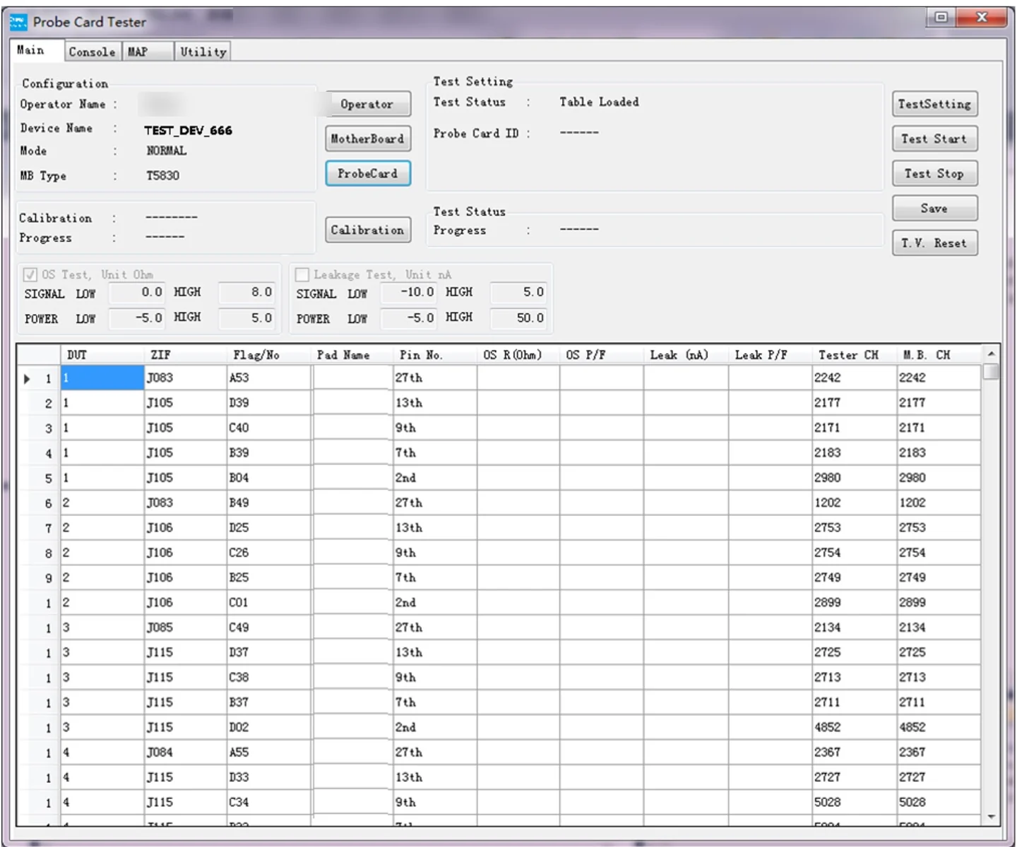
Screenshot of the tester's main screen: a per-needle table of DUT, ZIF, pin position, open-circuit resistance and leakage current
The tester's main screen: every needle listed by DUT, ZIF and pin position, with an open-circuit and a leakage verdict each.
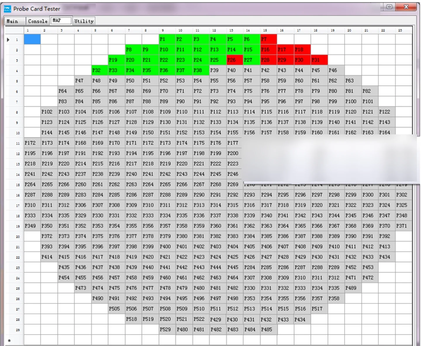
Screenshot of a whole-wafer result map: a 29-row die grid in green for pass and red for fail, with a hover panel showing needle and channel
The whole-wafer result map: green passes, red fails; open one cell and you see which needles sit under that die and which tester channel each one reaches.
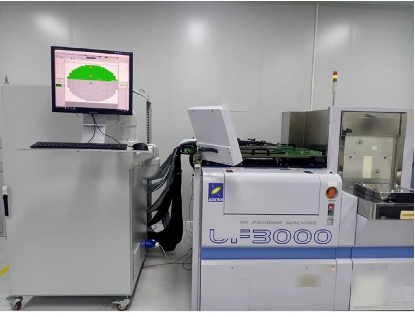
Photograph of an installation: the tester cabinet standing beside a 300 mm prober, with the whole-wafer result map on the screen next to it
On site: the tester cabinet stands beside the prober, with the whole-wafer result on the screen next to it.

PCT5801 Probe Card Test System

Full specification and process

Specifications

Maximum pinsPCT5801 67,000; PCT5801v2 300,000v2 is the flagship configuration and adds PinForce and probe-tip XYZ
ATE resources256 pin per unit, up to 4 unitsConfigured for the target card and test items
Relay matrix1,024 channels per piece, up to 64 piecesChannel capacity scales with pin count
Motherboard interfaceZIF / POGO with Bridge BeamInterface form designed per customer card
Control resourcesRelay / FPGA / ASIC custom control; MCW (T5830 / T5833); SPI and I²C (M5 / M7)Control scheme matched to the tester platform
Analog testKelvin four-wire measurement with DPS device power supplyFor accurate analog measurement
Configurable resourcesCurrent module, source-measure unit, digital I/O, arbitrary waveform generator and digitizer, signal capture moduleSelected per test item
Virtual instrumentsSource and measure, digitizer, scope and spectrum analysis, pin-map visualisationSoftware instrument panels
Operator interfaceGraphical, customisable GUITest flow and display adapt to customer practice
Time basisAbout 2 minutes for a simple open/short, 10 minutes for all pins, 20 minutes for pin-to-pin open/shortExcludes loading and temperature settling; varies with pin count and configuration
Leakage itemsPin-to-pin, pin-to-ground and relay open/closed-state leakage (front and rear relays distinguished); about 30 minutes for IO pinsDPS pin time depends on the capacitance connected
Resource expansionUp to 14 TRE (test resource extension) probe cardsDepends on the motherboard and card type
What a channel meansChannel counts are electrical signals on the tester side, not probe-card pinsKeeps channel counts from being read as pin counts
Digital capability16,384 channels delivered; 65,536 full-rack addressable ceiling; 200 MHz; 1.25 to 7 V; +/-32 mA; 128 M pattern memoryChannels are tester-side signals; 65,536 is the addressable full-rack ceiling, not simultaneous instrument resources
Measurement resourcesOne 18,600-pin configuration carries 256 PMU and 16 DPSA delivered configuration; varies per project
Software toolsGraphical sequence programmer, digital vector editor and debugger, logic analyser, virtual instrument panels, shmoo debugger, automatic VI-curve reportsSupplied with the system
Data and reportsProbe-card definitions in Excel (DUT map, signal definition, LBIO/MCW define), script-mode execution and automatic report generationFor recipe reuse and result archiving
Site conditionsAir cooled; 15 to 30 °C, 30 to 70 % RH; AC 220 V 50/60 HzNominal for the base configuration; varies with configuration
Control module GCM8 channels (I2C, SPI, JTAG and user protocols); 64 channels of relay controlConfigurable test resource
Analog VI source AVI6 channels, +/-64 V and +/-500 mAConfigurable test resource
Middle-power VI source MVI2 channels, +/-128 V and +/-2 AConfigurable test resource
High-voltage floating VI source HVI1 channel, 1000 V, 10 mA / 20 mA pulsedConfigurable test resource
Digital module DM32 digital pins with a 100 MHz PMU per pin, including 8 low-jitter pins (1 ps RMS typical) and 4 TMU channelsConfigurable test resource
Low-frequency AWG and digitizer LF4-channel AWG (200 ksps / 24 bit, 80 kHz bandwidth) and 4-channel digitizer (625 ksps / 24 bit, 200 kHz bandwidth)Configurable test resource
High-frequency AWG and digitizer HF2-channel AWG (512 Msps / 16 bit, 200 MHz bandwidth) and 2-channel digitizer (250 Msps / 16 bit, 200 MHz bandwidth)Configurable test resource
Signal capture SCAP4 channels to 2 Gsps; 500 MHz bandwidth on Pogo, 300 MHz on BNCConfigurable test resource

Evidence and record

Adapted tester platformsSolution adapted and delivered: Advantest T5830 (440/480), T5833 (520), V93000 and Teradyne Magnum 5. Solution in build: Advantest T5221, CCTech C16/P16/P16+, Teradyne UltraFlex. Solution planned: XB1152, TM8000, SM0X00, M7, T5825.
AC testThe PBDATA test measures transfer time (TDR) across all signal channels in about 20 minutes; total time varies with pin count and configuration.
Capability positionDelivers DC, AC (TDR), logic control and mechanical inspection together at ultra-high pin count; general probe card analyzers usually cover only part of this.
Where it has been shownShown as a working machine at Semicon China (Shanghai), Semicon Southeast Asia (Singapore) and SWTest (US) in 2025.
Where we standNo probe-card, ATE or OSAT capital behind us: the system is improved to what each probe-card maker asks for, with quality, cost and lead time set by contract.
Open the equipment page →

DeepTouch1000 Probe Station for Probe Card Test

Full specification and process

Specifications

Chuck force1000 kgf (about 9.81 kN)Whole-card validation of a high-pin-count card needs more than 450 kgf
Maximum pins300,000Configured for the target card and motherboard
StructurePB5801 all-in-oneProbe station integrated with the probe card test system
Load portMedia Loader PortCarrier in/out and sorting through the loader port
Force displayChuckForce DisplayLive chuck-force readout during touchdown
Device handlingHBM handlingHandling and alignment for high-stack devices
Tip inspection3D probe-tip XYZTip length, position deviation and planarity scanning
TemperatureTri-temperature (option)Range set by configuration and test conditions
POST unit (option)PinForce measurement and contact checkPressure sensor resolution 2 g, full scale 200 g, probe positioning accuracy 0.3 μm
Main body dimensions1320 × 1930 × 1500 mmNominal dimensions from specification RevA1
VibrationHigh-performance isolation platformSuppresses external vibration during tip measurement
Motion controlXY control resolution 40 nm; Z accuracy ±2 µm with 0.1 µm control resolutionSpecification RevA1
Tip imaging resolutionX/Y 0.345 µm; Z 0.5 µmThree-dimensional probe tip inspection optics
Card compatibilityVertical, cantilever and MEMS probe cardsAccepts 4.5 / 9 / 12 inch cards
Card alignment rangeX ±164 mm; Y 160 mm front, 130 mm rear3D imaging range 80 mm to the rear
Wafer300 mmAutomatic probe card exchange cart is optional
Temperature systemChuck surface −55 °C to 200 °C (system range −55 to +180 °C)Electric heating with CDA cooling; RevA1 specification, configuration lists differ - confirmed per project
XY/theta travel and accuracyXY accuracy +/-2 um; X +/-163 mm, Y +280 / -165 mm; up to 600 mm/sRevA1 specification
Z travel and contact window81.5 mm travel; contact set between 59.2 and 79.0 mm; up to 5 mm/s; +/-2 um overshootSetting window under the full 1000 kgf load
Chuck flatness15 um between 20 and 50 °C; 30 um between 50 and 200 °CBanded by temperature - the critical figure for full-card touchdown
Chuck electricalLeakage < 20 pA at 25 °C/10 V, < 30 pA at 200 °C/10 V; test voltage to 500 V300 mm chuck assembly figures, confirmed with the temperature option
Mass and site conditions2,000 kg; 25 °C +/-3 °C, humidity <= 65 %; floor vibration frequency >= 10 Hz recommendedInstallation conditions to check when choosing a site
UtilitiesSingle-phase AC 200/220/230/240 V three-wire, 50/60 Hz; 20 ms ride-through; 2.3 kVARevA1 specification
Standard softwareLive wafer map (PASS/FAIL/BIN, two-colour or multi-colour), manual inspection, offline recipe editing, log and result exportStandard configuration
Operator interfaceColour LCD 1920 x 1080, Chinese/English, touch operation with a visual test flowThe specification quotes two different screen sizes, so only resolution and languages are stated
SafetyEMO cuts power directly; head plate and loader side cover interlocked (including the optional WAPP door)Machine safety hardware; this is not a compliance claim
Tip inspection speedAbout 20 pin/s optical and 50 pin/s electrical; roughly 10 minutes for 10,000 pinsEstimate, to be confirmed per project
Z straightness under full load< 0.2 um from 0 to 1000 kgfMeasured under stepped loading; linearity is good
Chuck flatness under full loadDeviation <= 10 um over a 3 mm strokeMeasured at full load, within design spec
Tilt under full loadAbout 0.003 degrees, roughly 16.2 um across 300 mmMeasured at full load and judged acceptable
Loading repeatabilityConsistent across three loadings; symmetric structure with no asymmetric deformationMeasured at full load
POST unit travelUp to 20 mm/s in Z, 80 mm stroke, 0.02 um linear-scale resolutionOptional unit with an interchangeable probe tip
Measured tip-inspection throughputAbout 9 minutes for 8,500 pins, about 65 minutes for 60,000 pinsLine scanning at about 12,000 scans per second
Cleanliness and airflowBuilt-in FFU / HEPA filtered laminar flowLimits particles in the test area reaching tips and contacts
Automatic mother-board exchangeManipulator with Z lift and horizontal arm, plus a multi-unit storage rackOptional; swaps between several mother boards

Evidence and record

Design rationaleAdapted to Accretech UF3000 / UF3000ex and TEL P-12XL probe stations; chuck force limits high-pin-count cards on those platforms, which is why the 1000 kgf dedicated machine was built.
Full-load rigidity, measuredAt 23 +/- 1 C, two dial gauges of 0.1 um resolution were read simultaneously with a laser collimator mounted on the frame beam, loading in steps to 1000 kgf along the 3/9 o'clock axis (270 mm apart) and the 6/12 o'clock axis, recording only after each step settled. Results: Z-axis straightness below 0.2 um, chuck flatness deviation within 10 um over a 3 mm stroke, tilt about 0.003 degrees, and three loadings in agreement with no asymmetric deformation. Producing 1000 kgf of chuck force is not the hard part; holding the geometry while that force is applied is. These figures speak to the second, which is what whole-card touchdown at 300,000 pins depends on.
Data linkageProbe-tip XYZ, load, images and verdicts map to PCT5801 anomaly channel coordinates for localisation and re-verification.
AcceptanceFixtures, algorithms, thresholds, repeatability and task time are confirmed item by item on real samples during FAT/SAT.
Open the equipment page →
The same points in words
PCT5801 Probe Card Tester (combined cell)
a 1000 kgf-chuck probe station below, with the card loaded on the head plate and mated from above by the motherboard's ZIF/POGO contact ring. Open, short, nA-level leakage and control-resource checks run through a relay matrix of 1,024 channels per board, up to 64 boards; continuous testing repeats the touchdown cycle, mapping load, contact state and failing-channel coordinates together.
Maximum pins
PCT5801 and the v2 flagship Target card scale, configuration-dependent
ATE resources
Full-function ATE front end
Relay matrix
Modular channel expansion
Card interface
Bridge Beam contact structure
Release and post-repair test
Check opens, shorts, leakage and control resources with a traceable report.
Pre-ATE interface validation
Verify motherboard, channel and basic electrical state before occupying a production tester.
High-channel expansion
Organize capacity around 1,024-channel modules and scale for the card and rack configuration.
Open test
Continuity across all channels with every pin open About 5 minutes
Short test
All pins on a short plate to detect channel-to-channel shorts About 5 minutes
Leakage test
All pin-to-pin measurement against a 10 nA test threshold About 60 minutes at 10,000 pins
Control test
MCW / FPGA / ASIC / I²C / SPI control-resource verification About 5–30 minutes
Chuck force
Whole-card touchdown at high pin count
Structure
Probe station and test system combined
Geometry
Length, position and planarity
High-pin-count card loading
Evaluate loading, total force and contact state for HBM and large probe card projects.
Tip position and consistency
Use XYZ data and images to locate offsets, planarity or contact differences.
Electrical anomaly review
Align PCT5801 anomalous coordinates with probe-tip, mark and load evidence.
Incoming probe-card verification
Check electrical performance, contact behaviour and tip consistency on cards as received, before they are released to the line.
Confirm card and fixture
Define card structure, datum, load range, inspection area and safety conditions.
Load and image
Apply the recipe and capture tip, contact or probe-mark images.
Analyze XYZ and load
Calculate position and load, then flag locations outside project limits.
Correlate electrical results
Link PCT5801 coordinates and judgements to a traceable retest conclusion.
Development

10 · Tip grinding and cleaning

Condition tips and clear residue

The card is run over a grinding plate along a set path to condition tip shape and height and to clear residue from the tips.

How it works

  1. card in
  2. grinding plate
  3. re-measure
  4. release
The same points in words
Tip grinding and cleaning
The drawing shows a generic industry configuration.
Production

11 · Cleaning and Three-Direction Reinspection

Clean or not is settled by the customer's own acceptance criteria

The card is cleaned by recipe with atomized IPA, controlled soft brushing and clean-gas blow-off with vacuum recovery of residue and particles, then re-imaged from three directions to judge residue, particles, bent probes and abnormal tip shape, with thresholds defined by the customer acceptance method.

DeliveryAtomized IPA
CleaningControlled soft brush
DryingClean gas
ReviewThree-direction images

How it works

  1. recipe clean
  2. dry
  3. three views
  4. pass or rework

What we take on

  • In-line maintenance
  • Repeated contamination
  • Standalone cleaning cell
  1. 01Identify and pre-inspect
  2. 02Recipe-controlled clean
  3. 03Three-direction reinspection
  4. 04Release or close the loop

Probe Card Cleaning and Three-Direction Reinspection

Full specification and process

Specifications

Fluid deliveryAtomized IPAFlow, spray envelope and material compatibility confirmed on samples
BrushingControlled soft-brush motion and contactBrush type, contact mode, cycle and count held in the recipe
Blow-offClean-gas blow-offGas conditions and stop criteria set by facility and samples
RecoveryVacuum recovery of residue and particlesInterfaces with the line exhaust and waste-liquid plan
Visual reinspectionThree-direction imaging and judgementParticle size, detection threshold and inspection area frozen by sample trials
Inspection itemsTip and shank particles, diameter / length / pitch, bent probes and abnormal geometryJudgement rules defined by the customer acceptance method
Card compatibilityCantilever and vertical probe cardsHolding, attitude and keep-out zones designed per card type
Changeover and serviceFast changeover, brush replacement, fixture service and poka-yokeConsumable life and service interval set from measured data
Cleanliness and ESDLocal cleanliness, splash and cross-contamination control; ESD-controlled contact partsTargets set to the customer cleanroom specification
TraceabilityCard ID / RFIDRecords card number, recipe, clean count, images, verdict and operator
DeploymentStandalone station or inline; can serve as a clean-and-inspect submodule inside a larger toolMechanical, electrical, communication and safety interlock boundaries defined per project
Result stateRelease / rework / reinspect / quarantineJudgement rules defined by the customer acceptance method

Evidence and record

Process parametersCleaning settings, particle detection, task time and review limits are established with the target probe and contamination samples.
Standard processAtomized IPA, controlled brushing, clean gas and three-direction reinspection are managed in one recipe.
Delivery scopeMaterial compatibility, recipes, judgement, task time and interfaces are defined in project documents and accepted in FAT/SAT.
Open the equipment page →
The same points in words
Delivery
Reduces unnecessary wetting and supports recipe control
Cleaning
Motion, contact and cycles are probe-defined
Drying
Creates a stable entry state for reinspection
Review
Records particles and residue
In-line maintenance
Run traceable cleaning, reinspection and release between test and storage.
Repeated contamination
Use review images to separate clean, rework and isolation states.
Standalone cleaning cell
Manage cleaning for different card types through Card ID/RFID, recipes and reports.
Identify and pre-inspect
Read Card ID/RFID and confirm card type, contamination area and permitted cleaning method.
Recipe-controlled clean
Execute atomized IPA, controlled brushing and clean-gas blowoff by recipe.
Three-direction reinspection
Capture images and judge residue, particles and anomalies against project limits.
Release or close the loop
Release to test/storage or route to rework, repeat inspection and isolation.
Production

12 · Traceable Storage and Handoff

Where every card has been, on record

Each card is RFID-bound and placed into an environment-controlled slot, with check-in, checkout, return and stocktake driven by WMS/EAP/MES tasks and handoff by manual, AMR, robot or OHT, while capacity and environmental targets are set per project.

EnvironmentNitrogen / ESD / cleanliness
IdentityRFID
InterfacesWMS / EAP / MES
HandoffManual / AMR / robot / OHT

How it works

  1. bind ID
  2. controlled
  3. on request
  4. return on record

What we take on

  • High-value card custody
  • Test and cleaning handoff
  • Automated factory handoff
  1. 01Receive and bind identity
  2. 02Controlled storage
  3. 03Task-driven issue
  4. 04Return and audit

Traceable Probe Card Storage System

Full specification and process

Specifications

Environmental controlNitrogen, ESD, cleanliness, temperature/humidity and alarmsTargets follow card type, facility and customer specification
RFIDCard identity, location, state, movement and inventoryBand, tag, read distance and cross-read prevention are established on site
System interfacesWMS, EAP and MESFields, access, heartbeat, retry, compensation and audit follow the interface agreement
HandoffManual, AMR, robot and OHTActions, interlocks, buffers and recovery follow site layout
CapacityModular storage locationsCard type, footprint, service space and expansion plan define capacity
Security and traceabilityAccess, role, alarm, operation and movement historyLevels and retention are written into project documents
PerformanceStore/retrieve takt and concurrent tasksEstablished through site flow and physical trials

Evidence and record

ConfigurationNitrogen, ESD, RFID, capacity and task time are set for the card and site conditions.
System scopeRFID, WMS/EAP/MES and manual or automated handoff use one set of states and history.
AcceptanceInterface communication, exception recovery, environmental alarms and physical material flow are verified in FAT/SAT.
Open the equipment page →
The same points in words
Environment
Targets and alarms are project-defined
Identity
Links card, location, state and history
Interfaces
Fields, access and retry confirmed on site
Handoff
Designed individually or in combination
High-value card custody
Control environment and retain location, issue, return and exception history.
Test and cleaning handoff
Relate reinspection release, storage state and the next process task.
Automated factory handoff
Define task and state loops with WMS/EAP/MES and AMR/OHT/robot systems.
Receive and bind identity
Read or bind RFID and verify card, state, clean/test result and target location.
Controlled storage
Execute environment, access, location and handoff interlocks and record the outcome.
Task-driven issue
Receive WMS/EAP/MES or manual tasks and complete retrieval and downstream handoff.
Return and audit
Write back state, location, exception and operation history for inventory and traceability.
Not supplied

13 · Rework and Re-Pinning

Strip and re-weld probes

Cards returned from the fab have damaged or bent probes removed from the substrate and replacement probes welded in before re-entering metrology and electrical test; Probing's cleaning equipment only routes a card to a rework state and its test systems only re-test after repair, so the re-pinning itself is not supplied.

How it works

  1. find it
  2. remove
  3. re-weld
  4. re-check
Not supplied

14 · Packing and Shipment to Fab

Case, document and ship

The released card is put into its shipping case with desiccant and shock protection, documented, and transported to the customer fab's incoming dock.

How it works

  1. final check
  2. pack
  3. with its record
  4. ship
The same points in words
Packing and Shipment to Fab
Probing's storage system covers in-plant checkout and downstream handoff only, so packing and shipment are not supplied.

Within this room, probe fabrication, incoming sorting, space transformer and PCB fabrication, guide-plate machining, card body integration, packing and shipment, and re-pinning are handled by specialist suppliers, and the equipment for those steps sits outside Probing's supply scope. Every station marked as ours is marked only from what the product pages on this site already state.

Share the card, interfaces and target

Send the sample, installed equipment, current issue and target takt. We will acknowledge receipt within one business day.

Submit a request