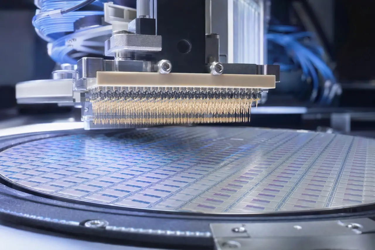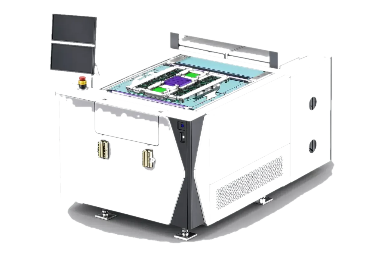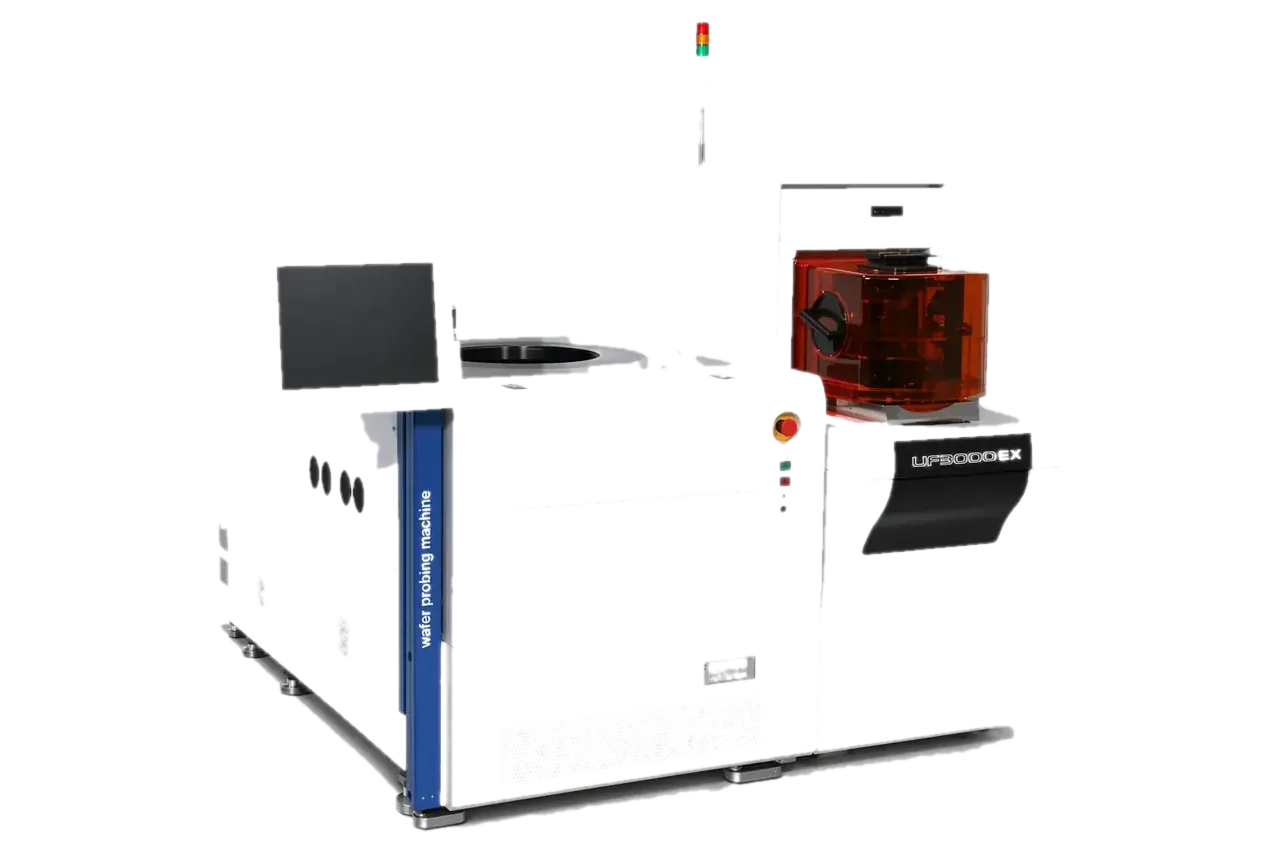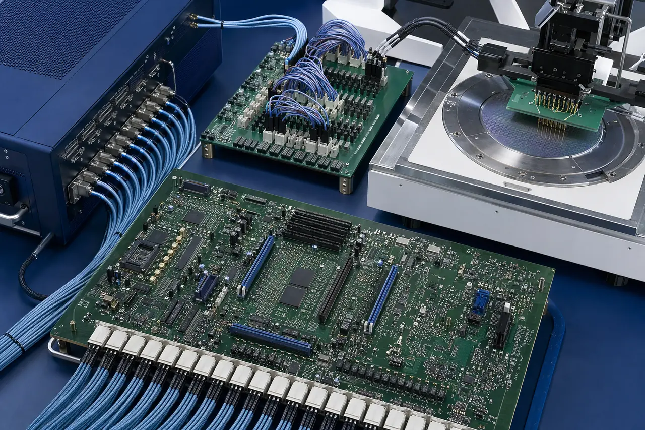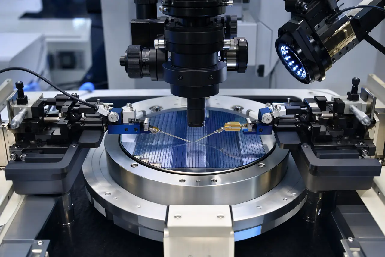
Probing Semiconductor
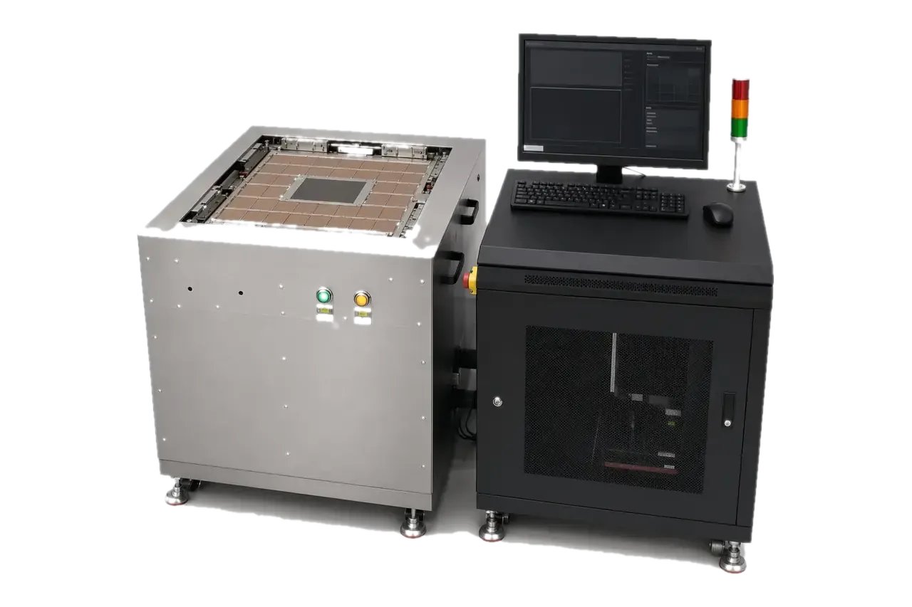
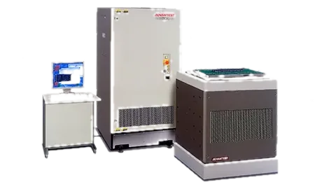
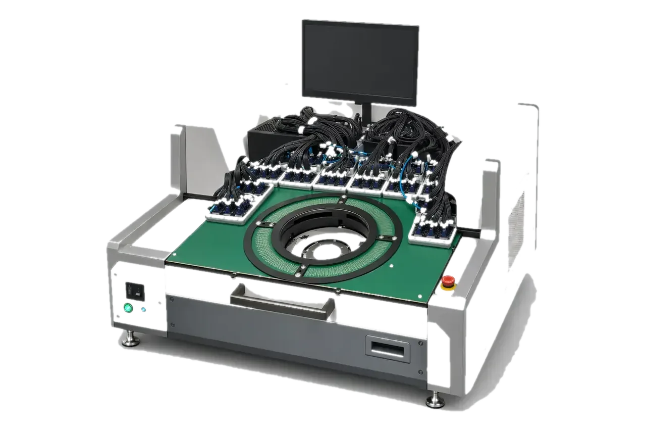
Mother board platforms for T5830 / T5833, M5, 93K, and real probe-card test workflows.
Mother board paths around T5830 / T5833, M5, and 93K sit together with PCT5801, DeepTouch1000, socket test, and broader semiconductor test workflows for production-side validation.