
Product
Memory probe card test for the HBM era.
This workflow is built around one-touchdown memory probe card test, high pin counts, tester-side realism, and an integrated electrical plus physical validation path.
This workflow is built around one-touchdown memory probe card test, high pin counts, tester-side realism, and an integrated electrical plus physical validation path.
This one-touchdown probe card test workflow is built to simulate actual mass-production wafer test conditions rather than act as a generic analyzer.
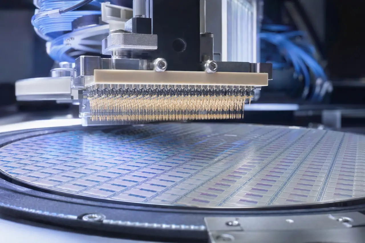
Targets NAND / NOR / DRAM memory tester workflows where pin count can move from 16,000 to 60,000 and further toward 300,000 in HBM-style contexts.
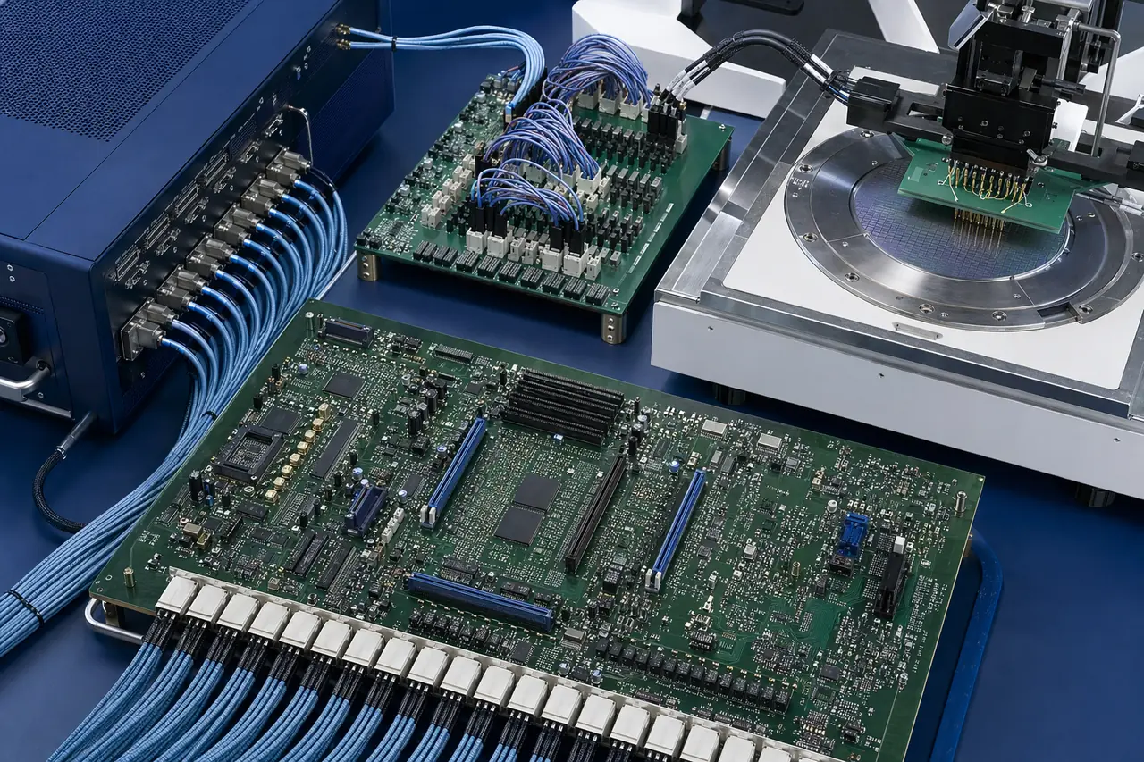
Relay, FPGA, ASIC, MCW, SPI, and I²C related control checks are part of the intended workflow rather than side tasks.
The design concept is explicit: build a probe card test system that fits tester, prober, and test-interface environments and helps customers solve real problems first.
The same workflow extends into the physical side through DeepTouch1000, where contact performance, tip consistency, and wafer-sort handling matter.
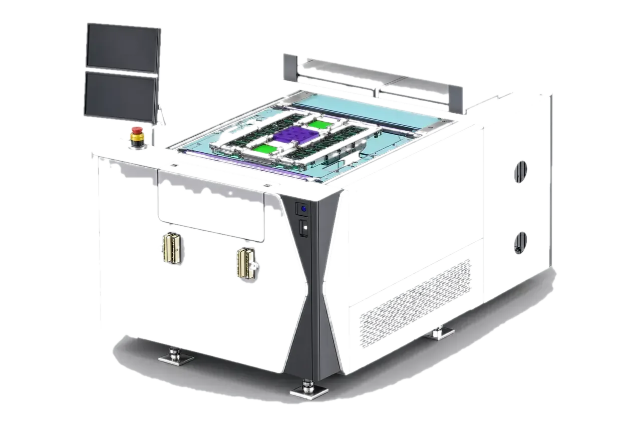
PB5801 all-in-one operation combines with 1000 kgf chuck force and needle-tip inspection support.
Supported probers include UF3000, UF3000ex, TEL Precio, SEMICS OPUS3, and CNS.
The product shape comes from long-term application experience around testers, probers, and test interfaces, with a strong problem-first bias.